LOW FREQUENCY TRANSISTOR AMPLIFIERS. POWER AMPLIFIERS
At the request of site visitors, I present to your attention an article completely devoted to transistor amplifiers. In the 8th lesson, we touched a little on the topic of amplifiers - amplifier stages on transistors, so with the help of this article, I will try to eliminate all the gaps in relation to transistor amplifiers. Some of the theoretical foundations presented here are valid for both transistor amplifiers and tube amplifiers. At the beginning of the article, the main types and methods of switching on the amplifier stages will be reviewed, at the end of the article we will consider the main pros and cons of single-ended transformer and transformerless amplifiers, and we will take a particular look at push-pull transformer and transformerless amplifiers, since they are often used and represent a large interest. At the end of the article, as in the previous lessons, there will be practical work. Actually, this article is no different from the lessons, with the only difference that this and all subsequent articles will have specific titles, which allows you to choose a topic for study at will. In any case, in order to safely choose any of the following topics, you must definitely complete the full course consisting of 10 lessons.
Amplifying transistor stage it is customary to call a transistor with resistors, capacitors and other parts that provide it with working conditions as an amplifier. For loud reproduction of audio frequency oscillations, the transistor amplifier must be at least two - three-stage ... In amplifiers containing several stages, stages are distinguished pre-amplification and output, or terminal, stages ... The last stage of the amplifier, which operates on telephones or a dynamic head of the loudspeaker, is called the output stage, and all the stages in front of it are called the preliminary stages. The task of one or more of the preamplification stages is to increase the audio frequency voltage to the value necessary for the operation of the output stage transistor. From the transistor of the output stage, an increase in the power of the audio frequency oscillations is required to the level necessary for the operation of the dynamic head. For the output stages of the simplest transistor amplifiers, radio amateurs often use low-power transistors, the same as in the pre-amplification stages. This is explained by the desire to make amplifiers more economical, which is especially important for portable battery-powered designs. The output power of such amplifiers is small - from several tens to 100 - 150 mW, but it is also enough for the operation of telephones or low-power dynamic heads. If the issue of saving energy of power supplies is not so significant, for example, when powering amplifiers from an electric lighting network, powerful transistors are used in the output stages. How does a multi-stage amplifier work? You can see the diagram of a simple transistor two-stage LF amplifier in (Fig. 1). Consider it carefully. In the first stage of the amplifier, transistor V1 operates, in the second, transistor V2. Here, the first stage is the preamp stage, the second is the output stage. Between them - decoupling capacitor C2. The principle of operation of any of the stages of this amplifier is the same and similar to the principle of operation of a single-stage amplifier you are familiar with. The only difference is in the details: the load of the transistor V1 of the first stage is the resistor R2, and the load of the transistor V2 of the output stage is the phones B1 (or, if the output signal is strong enough, the loudspeaker head). The bias to the base of the transistor of the first stage is fed through the resistor R1, and to the base of the transistor of the second stage through the resistor R3. Both stages are powered from a common Ui.p. source, which can be a battery of galvanic cells or a rectifier. The operating modes of the transistors are set by selecting the resistors R1 and R3, which is indicated in the diagram with asterisks.
Rice. 1 Two-stage transistor amplifier.
The overall effect of the amplifier is as follows. The electrical signal supplied through the capacitor C1 to the input of the first stage and amplified by the transistor V1, from the load resistor R2 through the blocking capacitor C2 is fed to the input of the second stage. Here it is amplified by the transistor V2 and the telephones B1, connected to the collector circuit of the transistor, are converted into sound. What is the role of the capacitor C1 at the input of the amplifier? It performs two tasks: it freely passes an alternating signal voltage to the transistor and prevents the base from shorting to the emitter through the signal source. Imagine that there is no such capacitor in the input circuit, and the source of the amplified signal is an electrodynamic microphone with a low internal resistance. What happens? Through the low resistance of the microphone, the base of the transistor will be connected to the emitter. The transistor will close as it will operate without an initial bias voltage. It will only open on negative half-cycles of the signal voltage. And the positive half-periods, which even more cover the transistor, will be "cut off" by it. As a result, the transistor will distort the amplified signal. Capacitor C2 connects the amplifier stages in alternating current. It should pass well the AC component of the amplified signal and delay the DC component of the collector circuit of the first stage transistor. If, together with the variable component, the capacitor also conducts direct current, the operating mode of the output stage transistor will be disrupted and the sound will become distorted or completely disappear. Capacitors that perform such functions are called coupling capacitors, transient or separating ... The input and transition capacitors must pass well the entire frequency band of the signal being amplified - from the lowest to the highest. This requirement is met by capacitors with a capacity of at least 5 μF. The use of large-capacity coupling capacitors in transistor amplifiers is explained by the relatively low input impedances of the transistors. The coupling capacitor provides the alternating current with a capacitive resistance, which will be the less, the larger its capacitance. And if it turns out to be greater than the input resistance of the transistor, a part of the AC voltage will drop across it, which is greater than the input resistance of the transistor, which will result in a loss in amplification. The capacitance of the coupling capacitor must be at least 3 to 5 times less than the input resistance of the transistor. Therefore, capacitors of large capacities are placed at the input, as well as for communication between the transistor stages. Small electrolytic capacitors are usually used here, with the obligatory observance of the polarity of their inclusion. These are the most characteristic features of the elements of a two-stage transistor LF amplifier. To fix the principle of operation of a transistor two-stage LF amplifier in memory, I propose to assemble, set up and test in action the simplest options for amplifier circuits below. (At the end of the article, options for practical work will be proposed, now you need to assemble a model of the simplest two-stage amplifier in order to quickly track theoretical statements in practice).
Simple, two-stage amplifiers
The schematic diagrams of two variants of such an amplifier are shown in (Fig. 2). They are, in essence, a repetition of the circuit of the now disassembled transistor amplifier. Only on them are the details of the parts indicated and three additional elements are introduced: R1, СЗ and S1. Resistor R1 - load of the audio frequency oscillation source (detector receiver or pickup); СЗ - capacitor that blocks the head B1 of the loudspeaker at the highest sound frequencies; S1 - power switch. In the amplifier in (Fig. 2, a) transistors of the p - n - p structure operate, in the amplifier in (Fig. 2, b) - structures n - p - n. In this regard, the polarity of switching on the batteries supplying them is different: negative voltage is applied to the collectors of transistors of the first version of the amplifier, and positive voltage is applied to the collectors of transistors of the second version. The polarity of switching on electrolytic capacitors is also different. The rest of the amplifiers are exactly the same.

Rice. 2 Two-stage LF amplifiers on transistors of the p - n - p structure (a) and on transistors of the n - p - n structure (b).
In any of these variants of the amplifier, transistors with a static current transfer coefficient h21e 20 - 30 and more can work. A transistor with a large coefficient h21e must be put in the preliminary amplification stage (the first) - The role of the load B1 of the output stage can be performed by headphones, a DEM-4m telephone capsule. To power the amplifier, use a 3336L battery (popularly called a square battery) or power supply unit(which was suggested to be made in the 9th lesson). Pre-assemble the amplifier on breadboard , and then transfer its details to the printed circuit board, if such a desire arises. First, mount only the first stage parts and capacitor C2 on the breadboard. Connect the headphones between the right (according to the diagram) terminal of this capacitor and the grounded conductor of the power supply. If now the input of the amplifier is connected to the output sockets for example: a detector receiver tuned to a radio station, or any other source of a weak signal is connected to it, the phones will receive the sound of a radio transmission or the signal of the connected source. Selecting the resistance of the resistor R2 (just as when adjusting the operating mode of a single-transistor amplifier, what I talked about in the 8th lesson ), use the loudest volume. In this case, the milliammeter included in the collector circuit of the transistor should show a current equal to 0.4 - 0.6 mA. With a supply voltage of 4.5 V, this is the most advantageous mode of operation for this transistor. Then mount the details of the second (output) stage of the amplifier, connect the phones to the collector circuit of its transistor. Phones should now sound significantly louder. Even louder, perhaps they will sound after the selection of resistor R4 will set the collector current of the transistor to 0.4 - 0.6 mA. You can do differently: mount all the parts of the amplifier, select the resistors R2 and R4 to set the recommended transistor modes (according to the collector circuit currents or voltages on the transistor collectors) and only after that check its operation for sound reproduction. This way is more technical. And for a more complex amplifier, and you will have to deal mainly with such amplifiers, it is the only correct one. I hope you understand that my advice for setting up a two-stage amplifier applies equally to both options. And if the current transfer ratios of their transistors are approximately the same, then the sound volume of phones - amplifier loads should be the same. With a DEM-4m capsule, the resistance of which is 60 Ohm, the quiescent current of the cascade transistor must be increased (by reducing the resistance of the resistor R4) to 4 - 6 mA. The schematic diagram of the third version of the two-stage amplifier is shown in (Fig. 3). A feature of this amplifier is that in its first stage, the transistor of the p - n - p structure operates, and in the second - the n - p - n structure. Moreover, the base of the second transistor is connected to the collector of the first not through a transition capacitor, as in the amplifier of the first two options, but directly or, as they say, galvanically. With such a connection, the range of frequencies of the amplified oscillations expands, and the mode of operation of the second transistor is determined mainly by the mode of operation of the first, which is set by selecting the resistor R2. In such an amplifier, the load of the transistor of the first stage is not the resistor R3, but the emitter p - n junction of the second transistor. The resistor is needed only as a bias element: the voltage drop created across it opens the second transistor. If this transistor is germanium (MP35 - MP38), the resistance of the resistor R3 can be 680 - 750 Ohm, and if it is silicon (MP111 - MP116, KT315, KT3102) - about 3 kOhm. Unfortunately, the stability of such an amplifier when the supply voltage or temperature changes is not high. Otherwise, everything that is said in relation to the amplifiers of the first two options applies to this amplifier as well. Can the amplifiers be powered from a 9 V DC source, for example, from two 3336L or Krona batteries, or, conversely, from a 1.5 - 3 V source - from one or two elements 332 or 316? Of course, you can: at a higher voltage of the power supply, the load of the amplifier - the loudspeaker head - should sound louder, at a lower voltage - quieter. But at the same time, the operating modes of the transistors should also be somewhat different. In addition, with a power supply voltage of 9 V, the nominal voltages of the electrolytic capacitors C2 of the first two amplifier options should be at least 10 V. While the amplifier parts are mounted on the breadboard, all this is easy to verify empirically and draw the appropriate conclusions.

Rice. 3 Amplifier on transistors of different structures.
It is not difficult to mount the parts of an adjusted amplifier on a permanent board. For example, (Fig. 4) shows the circuit board of the amplifier of the first option (according to the diagram in Fig. 2, a). Cut the board out of sheet getinax or fiberglass with a thickness of 1.5 - 2 mm. Its dimensions shown in the figure are approximate and depend on the dimensions of the parts you have. For example, in the diagram, the power of the resistors is indicated as 0.125 W, the capacitance of electrolytic capacitors is 10 μF each. But this does not mean that only such parts should be installed in the amplifier. The dissipation powers of the resistors can be anything. Instead of electrolytic capacitors K5O - 3 or K52 - 1 shown on the circuit board, there can be capacitors K50 - 6 or imported analogs, moreover, for high rated voltages. The amplifier PCB may change depending on the parts you have. You can read about the methods of mounting radioelements, including printed wiring, in the section "radio amateur technology" .

Rice. 4 Circuit board for two-stage bass amplifier.
Any of the amplifiers that I talked about in this article will be useful to you in the future, for example, for a portable transistor receiver. Similar amplifiers can be used for wired telephone communication with a friend living nearby.
Stabilization of the transistor operating mode
The amplifier of the first or second options (according to the diagrams in Fig. 2), mounted and adjusted indoors, will work better than outdoors, where it will be under the hot rays of the summer sun or in winter in the cold. Why does this happen? Because, unfortunately, with an increase in temperature, the operating mode of the transistor is violated. And the primary reason for this is the uncontrolled reverse collector current Ikbo and the change in the static current transfer coefficient h21E when the temperature changes. In principle, the current Ikbo is small. In low-frequency low-power germanium transistors, for example, this current, measured at a reverse voltage at the collector p - n junction of 5 V and a temperature of 20 ° C, does not exceed 20 - 30 μA, and for silicon transistors it is less than 1 μA. But it changes significantly when exposed to temperature. With an increase in temperature by 10 ° C, the current Ikbo of the germanium transistor approximately doubles, and that of the silicon transistor - 2.5 times. If, for example, at a temperature of 20 ° C, the current Ikbo of a germanium transistor is 10 μA, then when the temperature rises to 60 ° C, it increases to about 160 μA. But the current Ikbo characterizes the properties of only the collector p - n junction. In real operating conditions, the voltage of the power supply is applied to two p - n junctions - collector and emitter. In this case, the reverse collector current also flows through the emitter junction and, as it were, amplifies itself. As a result, the value of the uncontrolled current, changing under the influence of temperature, increases several times. And the greater its share in the collector current, the more unstable the operation of the transistor in different temperature conditions. An increase in the current transfer coefficient h21E with temperature increases the instability. What happens in this case in the cascade, for example, on the transistor V1 of the amplifier of the first or second options? As the temperature rises, the total collector current increases, causing an increasing voltage drop across the load resistor R3 (see Fig. 3). At the same time, the voltage between the collector and the emitter decreases, which leads to the appearance of signal distortions. As the temperature rises further, the collector voltage can become so low that the transistor will no longer amplify the input signal at all. Reducing the effect of temperature on the collector current is possible either by using transistors with a very low current Ikbo in equipment designed to work with significant temperature fluctuations. for example, silicon, or the use of special measures that thermally stabilize the mode of transistors. One of the methods thermal stabilization of the operating mode a germanium transistor of the p - n - p structure is shown in the diagram in Fig. 5, a. Here, as you can see, the base resistor Rb is connected not to the negative conductor of the power supply, but to the collector of the transistor. What does it do? With increasing temperature, the increasing collector current increases the voltage drop across the load Rн and decreases the voltage across the collector. And since the base is connected (through the resistor Rb) to the collector, the negative bias voltage also decreases on it, which in turn reduces the collector current. Feedback is obtained between the output and input circuits of the stage - the increasing collector current decreases the voltage at the base, which automatically reduces the collector current. The preset operating mode of the transistor is stabilized. But during the operation of the transistor between its collector and the base of the cheroz, the same resistor Rb appears negative AC feedback, which reduces the overall gain of the cascade. Thus, the stability of the transistor mode is achieved at the cost of gaining loss. It's a pity, but you have to go for these losses in order to maintain the normal operation of the amplifier when the temperature of the transistor changes.

Rice. 5 Amplifier stages with thermal stabilization of the transistor mode.
There is, however, a way to stabilize the operating mode of the transistor with slightly lower gain losses, but this is achieved by complicating the stage. The diagram of such an amplifier is shown in (Fig. 5, b). The quiescent mode of the transistor for direct current and voltage remains the same: the collector circuit current is 0.8 - 1 mA, the negative bias voltage at the base relative to the emitter is 0.1 V (1.5 - 1.4 = 0.1 V). But the mode is set using two additional resistors: Rb2 and Re. Resistors Rb1 and Rb2 form a divider with the help of which a stable voltage is maintained on the base. The emitter resistor Re is an element thermal stabilization ... Thermal stabilization of the transistor mode is as follows. As the collector current increases under the influence of heat, the voltage drop across the resistor Re increases. In this case, the voltage difference between the base and the emitter decreases, which automatically reduces the collector current. It turns out the same feedback, only now between the emitter and the base, thanks to which the transistor mode is stabilized. Cover the capacitor Ce connected in parallel with the resistor Re and, therefore, bypassing it with paper or a finger. What does this diagram remind you now? A stage with an OK transistor (emitter follower). This means that during the operation of the transistor, when a voltage drop across the resistor Re occurs, not only constant, but also variable components, there is between the emitter and the base 100% negative AC voltage feedback , at which the gain of the stage is less than unity. But this can only happen when there is no capacitor C3. This capacitor creates a parallel path along which, bypassing the resistor Re, there is an alternating component of the collector current, pulsating with the frequency of the amplified signal, and negative feedback does not arise (the alternating component of the collector current goes into the common wire). The capacitance of this capacitor should be such that it does not offer any appreciable resistance to the lowest frequencies of the amplified signal. In the audio frequency amplification stage, this requirement can be met by an electrolytic capacitor with a capacity of 10 - 20 μF or more. An amplifier with such a system for stabilizing the transistor mode is practically insensitive to temperature fluctuations and, in addition, which is no less important, to changing transistors. Is this how the transistor should be stabilized in all cases? Of course not. After all, it all depends on the purpose for which the amplifier is intended. If the amplifier will only work at home, where the temperature difference is insignificant, rigid thermal stabilization is not necessary. And if you are going to build an amplifier or receiver that would work stably both at home and on the street, then, of course, you need to stabilize the mode of the transistors, even if the device has to be complicated with additional details.
Push-pull power amplifier
Speaking at the beginning of this article about the purpose of the amplifier stages, I, as if running ahead, said that in the output stages, which are power amplifiers, radio amateurs use the same low-power transistors as in the voltage amplification stages. At that time, naturally, a question might have arisen in you, or it might have arisen: how is this achieved? I am answering it now. These stages are called push-pull power amplifiers. Moreover, they can be transformer, i.e. using transformers in them, or transformerless. Your designs will use both types of push-pull audio frequency amplifier. Let's figure out the principle of their work. A simplified diagram of a push-pull transformer power amplification stage and graphs illustrating its operation are shown in (Fig. 6). As you can see, it contains two transformers and two transistors. Transformer T1 is interstage, connecting the pre-final stage with the input of the power amplifier, and transformer T2 is the output. Transistors V1 and V2 are connected according to the OE circuit. Their emitters, like the middle terminal of the secondary winding of the interstage transformer, are "grounded" - connected to the common conductor of the power supply Ui.p. - negative supply voltage to the collectors of transistors is supplied through the primary winding of the output transformer T2: to the collector of transistor V1 - through section Ia, to the collector of transistor V2 - through section Ib. Each transistor and the related sections of the secondary winding of the interstage transformer and the primary winding of the output transformer represent the usual single-ended amplifier you are already familiar with. This is easy to see if you cover one of these cascade arms with a piece of paper. Together they form a push-pull power amplifier.

Rice. 6 Push-pull transformer power amplifier and graphs illustrating its operation.
The essence of the push-pull amplifier is as follows. Oscillations of the audio frequency (graph in Fig. 6) from the pre-final stage are fed to the bases of both transistors so that the voltages across them change at any time in opposite directions, ie. in antiphase. In this case, the transistors operate alternately, for two cycles for each period of the voltage supplied to them. When, for example, on the base of transistor V1 there is a negative half-wave, it opens and only this transistor current flows through section Ia of the primary winding of the output transformer (graph b). At this time, the transistor V2 is closed, since there is a positive half-wave of voltage on its base. In the next half-cycle, on the contrary, the positive half-wave will be at the base of the transistor V1, and the negative half-wave will be at the base of the transistor V2. Now transistor V2 opens and its collector current flows through section Ib of the primary winding of the output transformer (graph c), and transistor V1, closing, "rests". And so for each period of sound vibrations supplied to the amplifier. In the transformer winding, the collector currents of both transistors are summed up (graph d), as a result, more powerful electrical oscillations of the audio frequency are obtained at the output of the amplifier than in a conventional single-ended amplifier. Speaker B, connected to the secondary winding of the transformer, converts them into sound. Now, using the diagram in (Fig. 7), we will understand the principle of operation transformerless push-pull amplifier power. There are also two transistors, but they are of different structures: transistor Vl - p - n - p, transistor V2 - n - p - n. For direct current, the transistors are connected in series, forming, as it were, a voltage divider of the direct current source supplying them. In this case, on the collector of the transistor V1 relative to the midpoint between them, called the point of symmetry, a negative voltage is created equal to half the voltage of the power supply, and on the collector of the transistor V2 - positive, and also equal to half of the voltage of the power supply Un.p. Dynamic head B is included in the emitter circuits of transistors: for the transistor V1 - through the capacitor C2, for the transistor V2 - through the capacitor C1. Thus, the AC transistors are connected according to the OK circuit (emitter followers) and work for one common load - head B.

Rice. 7 Push-pull transformerless power amplifier.
At the bases of both transistors of the amplifier, an alternating voltage of the same value and frequency acts from the pre-final stage. And since the transistors are of different structures, they work alternately, for two cycles: with a negative half-wave of voltage, only transistor V1 opens and in the circuit head B - capacitor C2 a collector current pulse appears (in Fig. 6 - graph b), and with a positive half-wave opens only the transistor V2 and in the circuit head - capacitor C1 appears a pulse of the collector current of this transistor (in Fig. 6 - graph c). Thus, the total current of the transistors flows through the head (graph d in Fig. 6), which is amplified in power vibrations of the audio frequency, which it converts into sound vibrations. In practice, the same effect is obtained as in an amplifier with transformers, but due to the use of transistors of different structures, there is no need for a device for feeding a signal to the base of transistors. antiphase ... You may have noticed one contradiction in my explanation of push-pull power amplifiers: no bias voltages were applied to the bases of the transistors. You are right, but there is no particular mistake here. The point is that push-pull transistors can operate without an initial bias voltage. But then distortions of the type appear in the amplified signal "step" especially strongly felt when the input signal is weak. They are called a “step” because on the oscillogram of a sinusoidal signal they have a stepped shape (Fig. 8). The simplest way to eliminate such distortions is to apply a bias voltage to the bases of the transistors, which is what they do in practice.

Rice. 8 Distortion of the "Step" type.
Now, before we start talking about amplifiers that provide loud sound reproduction, I want to acquaint you with some parameters and amplification classes that characterize a bass amplifier. All the advantages of push-pull amplifiers will be discussed in detail below.
BASIC PARAMETERS OF LF AMPLIFIERS
The quality and suitability of an amplifier for certain purposes is judged by several parameters, the most important of which are three: output power Pout, sensitivity and frequency response. These are the basic parameters that you should know and understand. Output power is the power of the electrical vibrations of the audio frequency, expressed in watts or milliwatts, that the amplifier delivers to a load — usually a direct-radiating driver. In accordance with the established standards, a distinction is made between nominal Pnom and maximum power Pmax. The nominal power is such that the so-called nonlinear distortion of the output signal introduced by the amplifier does not exceed 3 - 5% with respect to the undistorted signal. As the power increases further, the harmonic distortion of the output signal increases. The power at which the distortion reaches 10% is called the maximum. The maximum output power can be 5 to 10 times the nominal, but distortion is noticeable even by ear. When I talk about amplifiers in this article, I will usually indicate their average output powers and simply refer to them as output powers. The sensitivity of the amplifier is the voltage of the audio frequency signal, expressed in volts or millivolts, which must be applied to its input so that the power at the load reaches its nominal. The lower this voltage, the naturally better the sensitivity of the amplifier. For example, I will say: the sensitivity of the overwhelming majority of amateur and industrial amplifiers intended for reproducing signals from the line output of a tape recorder, DVD player and other sources can be 100 - 500 mV and up to 1V, the sensitivity of microphone amplifiers is 1 - 2 mV. Frequency response - AFC (or the operating frequency band of the amplifier) is expressed graphically by a horizontal, somewhat curved line showing the dependence of the output signal voltage Uout on its frequency at a constant input voltage Uin. The fact is that any amplifier, for a number of reasons, amplifies signals of different frequencies unequally. As a rule, the vibrations of the lowest and highest frequencies of the audio range are amplified worst of all. Therefore, the lines - the frequency characteristics of the amplifiers - are uneven and necessarily have dips (blockages) at the edges. Oscillations of extreme low and high frequencies, the amplification of which in comparison with oscillations of medium frequencies (800 - 1000 Hz) falls to 30%, are considered the boundaries of the amplifier frequency band. The frequency band of amplifiers intended for reproducing musical works should be at least from 20 Hz to 20-30 kHz, amplifiers of network broadcasting receivers - from 60 Hz to 10 kHz, and amplifiers of small-sized transistor receivers - from about 200 Hz to 3-4 kHz. To measure the main parameters of amplifiers, you need an audio frequency oscillator, an alternating voltage voltmeter, an oscilloscope and some other measuring instruments. They are in production radio laboratories, radio electronics circles, and for more productive radio electronics, you need to try to get them for yourself, so that they are always at hand.
Classes of amplification of LF amplifiers. The role of the amplification class in achieving power parameters and high efficiency
Until now, we have not talked about how much energy is expended to create an amplified signal, to create a "powerful copy" of the input signal. We, in fact, did not have such a question. It must be said that the energy supplier for creating an amplified signal can be a battery or a power supply. In this case, it is considered obvious that the battery has large reserves of energy and there is nothing to spare it just to create an amplified signal. Now that the goal has been achieved, when we have learned to amplify a weak signal with the help of a transistor, we will try to find out what energy should be given by its supplier - a collector battery. Let's try to find out how much a watt of amplified signal costs, how many watts of DC power the battery has to pay for it. Having made a number of assumptions, assuming that the straight-line section of the input characteristic starts directly from "zero", that there are no bends on the output characteristic either, that an element (for example, a transformer) is included as a collector load, on which DC voltage is not lost, we come to the conclusion, that in the best case, only half of the power consumed from the battery goes into the amplified signal. This can be said differently: efficiency (efficiency) transistor amplifier does not exceed 50%. For every watt of output power you have to pay double the price, two watts of collector battery power (Figure 9).

Rice. 9 The higher the efficiency of an amplifier, the less power it consumes to create a given output power.
It is quite easy to prove the validity of this conclusion. To calculate the power consumed from the battery, you need to multiply its constant voltage Ek on the consumed current, that is, on the collector quiescent current Ic.p. ... transistor (Ppot. = Eк * Ic.p.) ... On the other hand, the amplitude of the variable component of the collector current can in no way be greater than the quiescent current, otherwise the transistor will operate with cutoff. In the best case, the amplitude of the variable component is equal to the quiescent current Ic.p. and the effective value of the variable component of the collector current is Iн.эф. = 07 * Ic.p .. In the same way, the amplitude of the alternating voltage across the load cannot be greater than the battery voltage, otherwise at some moments on the collector there will appear not a "minus", but a "plus". And this, at best, will lead to severe distortions. Thus, the effective value of the output voltage Un.eff. cannot exceed Un.eff. = 07 * Ek ... Now all that remains is to multiply 07 * Ic.p .. at 07 * EC. and get that the maximum effective power that the amplifier can deliver does not exceed Ref. = 0.5 * Ic.p. * Eк = W.eff. , that is, does not exceed half of the power consumption. The decision is final, but it is subject to appeal. It is possible, at the cost of certain sacrifices, to increase the efficiency of the amplifier, to cross the line of fifty percent efficiency. To increase the efficiency, it is necessary for the amplifier to create a more powerful signal with the same power consumption. And for this you need, without increasing the quiescent current Ic.p. and constant voltage Ek , increase the alternating components of the collector current Iн and load voltage Un. What prevents us from raising these two components? Distortion ... We can increase the current Iн (for this it is enough, for example, to increase the input signal level), and the voltage Uн (for this, it is enough, again, to increase the input signal or increase the load resistance for (alternating current). But in either case, the signal shape will be distorted, its negative half-waves will be cut off. And although such a sacrifice seems unacceptable (who needs an economical amplifier, if it gives out defective products?), we will still go for it.Firstly, because by allowing distortions (and then getting rid of them), we will be able to transfer the amplifier to a more economical mode and raise its efficiency. Amplification without distortion, when the amplitude of the variable component of the collector current does not exceed the quiescent current Ic.p., is called the gain class (A). A single amplifier operating in Class A is called a single ended amplifier. If during amplification a part of the signal is "cut off", if the amplitude of the variable component of the collector current is greater than Ic.p, and the current is cut off in the collector circuit, then we get one of the amplification classes (AB), (B) or (C). When amplified in class B, the cutoff is equal to the half-period, i.e. in half of the period there is current in the collector circuit, and in the other half of the period there is no current. If there is a current in more than half the period, then we have an AB amplification class, if it is less than a C class. (More often, the amplification classes are denoted by the Latin letters A, AB, B, C). Imagine that we have not one, but two identical amplifiers operating in class B: one reproduces positive half-periods of the signal, the other negative. Now imagine that both of them are working for a common load. In this case, we will receive a normal undistorted alternating current in the load - a signal, as it were, stitched together from two halves (Fig. 10).

Rice. 10 Push-pull stage and amplification classes.
True, to obtain an undistorted signal from two distorted ones, we had to create a relatively complex scheme for stitching the halves (such a scheme as discussed above in this article is called push-pull), in fact, consisting of two independent amplifying stages. But as already explained above, our loss (in this case, the complication of the amplifier circuit) brings a much greater gain. The total power that a push-pull amplifier develops is greater than the power that would be given separately by both halves of it. And the "cost" of one watt of the output signal turns out to be much less than in a single-ended amplifier. In the ideal case (key mode), one watt of the output signal can be obtained for the same watt of power consumption, that is, in the ideal case, the efficiency of a push-pull amplifier can reach 100 percent. The real efficiency is, of course, less: in practice, it is 67%. But after all, in a single-ended amplifier operating in the classroom A, we got an efficiency equal to 50%, also only in the ideal case. A really single-ended amplifier allows you to get an efficiency of no more than 30 - 40%. And therefore in a push-pull amplifier, each watt of output power costs us two to three times "cheaper" than in a single-ended one. For portable transistor equipment, an increase in efficiency is of particular importance. The higher the efficiency, the lower the energy consumption of the collector battery at the same output power. And this, in turn, means that the higher the efficiency, the less often this battery will need to be replaced or the smaller the battery can be with the same service life. That is why push-pull amplifiers are used in miniature transistor equipment, in particular in miniature receivers, where it would seem necessary to save weight and space, including a number of unnecessary parts in the circuit for this. Circuits of push-pull amplifiers for repetition will be given in practical work. Practically in all circuits of push-pull, transistor power amplifiers, class AB or B is used. However, when working in a class B some difficult-to-eliminate distortions appear (due to the bend in the input characteristic), and this class is used less often in low-frequency amplifiers. Class C is not used at all in these amplifiers due to the appearance of fatal distortion. The control voltage to the output transistors is supplied from the so-called phase-inverted stage , made on a transistor according to a transformer circuit. There are other schemes phase inverters , but they all perform the same task, create two antiphase voltages that must be applied to the bases of the push-pull transistors. If the same voltage is applied to these transistors, then they will not work through a cycle, but synchronously, and therefore both will amplify only positive or, conversely, only negative half-periods of the signal. In order for the transistors of the push-pull stage to work alternately, you need to feed them to their bases, as mentioned above antiphase voltages ... In a phase inverter with a transformer, two control voltages are obtained by dividing the secondary winding into two equal parts. And these voltages become antiphase because the middle point of the secondary winding is grounded. When a "plus" appears at its upper (according to the diagram) end relative to the midpoint, a "minus" appears at the lower end relative to this point. And since the voltage is variable, the "plus" and "minus" change places all the time (Fig. 11).

Rice. 11 The phase inverter produces two alternating voltages 180 degrees out of phase.
Transformer bass reflex simple and reliable, it practically does not need to be adjusted. A push-pull amplifier for a transistor receiver or a small radio can be assembled according to any of the LF amplifier circuits that will be given in practical work or industrial receiver circuits. For example, according to the scheme of receivers "Alpinist", "Neva-2", "Spidola", etc.
A little more detail on the negative feedback that was mentioned at the beginning of this article when describing single-ended amplifiers. How does negative feedback reduce distortion, correct the waveform? To answer this question, you need to remember that distortion of the waveform, in fact, means the appearance in the signal new harmonics , new sinusoidal components. Through the negative feedback loop, new ones that have appeared as a result harmonic distortion are fed to the input of the amplifier in such a phase (antiphase) that they weaken themselves. The power of these harmonics at the amplifier output turns out to be less than it would be without feedback. At the same time, of course, useful components are also weakened, from which an undistorted signal should be formed, but this is a fixable matter. To compensate for this harmful negative feedback activity, it is possible to increase the level of the signal entering the amplifier input, perhaps even adding another stage for this. Negative feedback in bass amplifiers, especially in push-pull amplifiers operating in classrooms AB and B, finds a very wide application: negative feedback allows you to do something that cannot be achieved by any other means, it allows reduce waveform distortion, reduce so-called harmonic distortion ... Negative feedback allows you to perform another important operation to adjust the tone, that is, in the desired direction change the frequency response of the amplifier Fig. 12 .

Rice. 12. An approximate graph of the amplitude-frequency response (AFC), amplifiers. A similar graph can be used to characterize the frequency response of any amplifier.
This characteristic shows how the gain changes with the frequency of the signal. For an ideal amplifier, the frequency response is just a straight line: the gain at all frequencies is the same for such an amplifier. But in a real amplifier, the frequency response is bent, overwhelmed in the region of the lowest and highest frequencies. This means that the low and high frequencies of the audio range are amplified worse than the mid frequencies. The reasons for the appearance of such blockages in the frequency response may be different, but they have a common root. Unequal gain at different frequencies is obtained because the circuit contains reactive elements, capacitors and coils, the resistance of which changes with frequency. There are many ways to correct the frequency response, including introduction of frequency - dependent elements into the feedback loop. An example of such elements is the chain R13, C9 in the amplifier shown in (Fig. 13).

Rice. 13 Practical design of a transformerless push-pull amplifier.
The resistance of this chain increases with decreasing frequency, the feedback decreases, and due to this, a certain rise in the frequency response in the region of lower frequencies is created. There are several more negative feedback circuits in the amplifier. This is the capacitor C6, which connects the collector of the transistor T2 to its base; resistor R12, which supplies not only a constant bias to the bases of the output transistors, but also some part of the output signal. A circuit that creates a feedback of the third stage with the second, but not in alternating current, but in direct current (such feedback increases the thermal stability of the amplifier). The dynamic head is connected to the collector circuits of the output transistors through a blocking capacitor C4. The resistance of the voice coil in this circuit can be 6 - 10 ohms. The amplifier develops power up to 100 mW. at an input signal voltage of about 30 - 50 mV. There are a fairly large number of transformerless amplifier circuits based on transistors of different conductivity. In most of them, composite transistors are used in the output stage, that is, two transistors are included in each arm. The absence of transformers and the reduction in the number of blocking capacitors allows such amplifiers to obtain a very good frequency response. However, for a novice radio amateur, this gain comes at a rather high price. Transformerless amplifiers, and even with composite transistors, are not always easy to establish. And therefore, if you still do not have much experience in setting up transistor equipment, it is better to assemble an amplifier according to the classic push-pull circuit with transformers (Fig. 14).

Rice. 14 Push-pull ULF with transformer output stage.
The main feature of this amplifier is the offset from a separate B2 battery to the base of the first stage T1. Due to this, the collector current of the transistor T1 remains practically unchanged when the voltage of the collector battery decreases down to 3.5 V. From the bottom of the divider R4, R5, included in the emitter circuit T1, a bias is applied to the bases of the transistors of the output stage. And therefore, with a decrease in the collector voltage, the bias of the transistors T2, T3 does not change. As a result, the amplifier operates at a reduced voltage, although with a lower output power (at 3.5V, 20 mW), but without distortion. The current consumed from the B2 battery does not exceed 500 μA. The amplifier has a simple tone control R6 and a feedback circuit R8, C8 that reduces distortion. Resistor R9 is necessary so that when B2 is turned off (it may happen that Bk2 will open the circuit some fractions of a second earlier than Bk1, the transistor T1 does not turn out to be with a "hanging base". Capacitors C7, C6 elements of negative feedback, preventing self-excitation at supersonic frequencies. The same task is performed by the capacitor C3. Transformers Tr1 and Tr2 are taken from the Alpinist receiver. Dynamic head with a voice coil resistance of about 4 - 6 ohms. With a collector voltage of 9 V. The amplifier develops a power of 180 mW. and consumes from battery B2, the current is not more than 20 - 25 mA. If you need to increase the output power, you can turn on powerful transistors as T2 and T3, for example P201. In this case, you need to halve R7 and select R5 so that the total collector quiescent current T2 and T3 was 15 - 25 mA. For powerful transistors, another output transformer is needed, for example, with the following data: a core with a cross section of about 3.5 cm2 (W17 x 17); primary winding 3 30 + 330 turns of PEV 0.31, secondary winding of 46 turns of PEV 0.51. With P201 transistors, the amplifier develops an output power of 1.52 - 2 W. The adjustment of all low-frequency amplifiers is reduced to the selection of transistor modes. For push-pull circuits, it is advisable to pre-select for both arms transistors with similar parameters: current gain and collector reverse current.If all parts are in good working order and the circuit is assembled correctly, then the amplifier, as a rule, starts working immediately. And the only serious trouble that can show up when you turn on the amplifier is self-excitation. One way to combat this is to introduce decoupling filters that prevent communication between the stages through the power supplies.
Practical work
In practical work, I want to present a few more simple amplifiers for repeating and consolidating the theoretical part of this article. The examples of push-pull amplifiers given at the end of the article are also quite suitable for repetition. These schemes, like many other drawings, are taken from literary sources of the 60s - 70s, but they have not lost their relevance. Why do you ask, am I using such outdated drawings? I will say there are at least 2 reasons: 1). There is catastrophically not enough time to draw them myself, although I still try to draw some of them. 2). Oddly enough, it is the drawings from the literature of the past, long forgotten years, that fully reflect the essence of the processes under study. Probably, it is not the pursuit of royalties, as is now customary, that affects the importance of high-quality presentation of the material. Yes, and censorship workers in those years, not in vain. ate their own bread.
So, instead of the transistors P13 - P16 indicated on the diagrams, you can use MP39 - 42, MP37, MP38 from silicon transistors, you can use KT315, KT361, respectively, pay attention to the type of conductivity and power of the transistors used. If the amplifier has powerful output transistors of the P213 - 215 type in the circuit, they can usually be replaced with silicon power transistors such as KT814 - 817 or KT805, KT837, observing the type of conductivity, respectively. In any case, when replacing germanium transistors with silicon ones, it is necessary to adjust the values of the resistors in the circuits of the transistors being replaced.

A simple transformerless push-pull amplifier with a power of 1.5 watts. The high-frequency transistor P416 is used here for reasons of reducing the noise of the input stage as much as possible, because in addition to being high-frequency, it is also low-noise. In practice, it can be replaced with MP39 - 42, with a deterioration in noise characteristics, respectively, or with silicon transistors KT361 or KT3107 with any letter .. used in detector receiver, due to which a bias voltage is formed at the bases of the transistors. The voltage at the midpoint (negative terminal of the capacitor C2) will be equal to 4.5v. It is set by selecting resistors R2, R4. The maximum allowable operating voltage of the capacitor C2 can be 6V.
More options for amplifiers, 1st, 2nd, available for repetition by novice radio amateurs, including silicon transistors. Variants of a pre-amplifier and a simple passive tone block are also shown. (opens in a separate window).
|Objective: Study of the operation of electronic amplifiers and their circuitry. Experimental and computer study of the OOS effect on the main characteristics of a low-frequency amplifier.
Introduction. Basic concepts
To increase the amplitude of the voltage or current, as well as the power of electrical signals, special devices are used, called electronic amplifiers.
All amplifiers can be divided into two classes - linear and non-linear.
For amplifiers with a linear mode of operation, requirements are imposed on obtaining an output signal close to the input signal in shape. Waveform distortion introduced by the amplifier should be kept to a minimum. This is achieved due to the proportional transfer of the instantaneous voltage and current values by the amplifier, which make up the input signal in time.
The most important indicator of amplifiers, as linear four-port networks with a linear mode of operation, is the complex voltage or current transfer ratio:
 .
.
 The magnitude
  is complex, i.e. characterizes the change in both the amplitude and the phase of the signal at the output of the amplifier in comparison with their values at the input. Amplifier gain module
  are called gain... The modulus of the complex gain versus the frequency determined for the harmonic input signal is frequency response(Frequency response) amplifier. Dependence of the argument of the complex transmission coefficient on frequency
  bears the name phase-frequency characteristics of the amplifier.
Depending on the type of frequency response, amplifiers with a linear mode of operation are divided into:
amplifiers of a slowly changing signal (DC amplifiers - DCA),
low frequency amplifiers (ULF),
high frequency amplifiers (UHF),
broadband, pulse amplifiers (silos),
selective, narrow-band amplifiers (UPA).
A characteristic feature of the UPT is the ability to amplify signals with a lower frequency approaching (f n 0). The upper limit of the frequency f in the DCA can be, depending on the purpose, 10 3 10 8 Hz. ULFs are characterized by a frequency range from tens of hertz to tens of kilohertz. UHF have a bandwidth from tens of kilohertz to tens and hundreds of megahertz. Silos - have a lower frequency limit about the same as that of the ULF, and the upper one - like the UHF. Linear pulse amplifiers are made on the basis of silos. UPU - characterized by the transmission of a narrow frequency band.

f in f f n f in f f n f in f f n f in f f o f
In amplifiers with a non-linear mode of operation, there is no proportionality in the transmission of instantaneous values of the input signal. Depending on the law of variation of the output signal from the input  , amplifiers with a nonlinear mode of operation include: amplifiers, limiters, logarithmic amplifiers, etc. power.
Let's consider the main parameters and characteristics of amplifiers.
Gain
.
Voltage gain  various amplifiers reaches tens of thousands. Often in order to achieve the necessary
  use multistage amplifiers in which
  the previous stage is
  for the following and the overall gain is:
The gain is a dimensionless value and in some cases it is customary to express the gain properties in logarithmic units - decibels:
 .
.
For a multistage amplifier:
They also use the current and power gain, which can also be expressed in decibels.
 .
.
Input and output impedance ... The amplifier can be considered as an active four-pole system, to the input terminals of which a source of the amplified signal with an EMF E in and an internal resistance is connected R W, and to the output - load resistance R N. For the output circuit, the amplifier is a source of EMF E out with an internal resistance R out.
For the amplified signal, the amplifier is characterized by an input impedance  ... Resistance R out is determined between the output terminals of the amplifier when the load is disconnected.
 R w R out I out = I n
E in U in R in E out U out R n
Amplifier
The current flowing from the signal source to the amplifier and the input voltage are determined by the formulas:
 .
.
Depending on the ratio between R W
and
R in
the signal source can operate in the following modes: a) idle, if R in> R w ,
when  ; b) short circuit if
R in< R вт
и
значит I вх
E вх
/
R вт ;
v)
matching, when R in R W and the maximum power is transmitted to the amplifier.
; b) short circuit if
R in< R вт
и
значит I вх
E вх
/
R вт ;
v)
matching, when R in R W and the maximum power is transmitted to the amplifier.
Amplifier power:

Equating to zero the derivative  , we get
  ... In this case, the amplifier receives
  , i.e. a quarter of the potential power of the signal source. Similar operating modes are possible for the output circuit.
When the load and the output impedance of the amplifier are matched, the greatest power is released in the load.
output power . With a purely resistive load and sinusoidal voltage

where  - effective and peak value of the output voltage;
  - the amplitude of the current in the load.
Efficiency
.
Efficiency  , where Р is the power consumed by the amplifier from the power sources.
It should be noted that any amplifier, no matter what type of energy it operates on, is, in essence, only a regulator for the power P out , transmitted from the power source to the load, and the input signal only regulates the value of this transmitted power, spending on this power P in .
Amplitude characteristic of the amplifier. The amplitude characteristic reflects the dependence of the output voltage amplitude on the change in the input voltage amplitude. This characteristic is used to judge the possible range of changes in the input and output signals of the amplifier. It is filmed with a harmonic input signal for the midrange.
A typical form of the amplitude characteristic is shown in the figure. Region 1-3 corresponds to proportional gain. The section below point 1 of the amplitude characteristic is not used, since the useful signal is difficult to distinguish from the intrinsic noise of the amplifier.
U  out. m .

U max 
 3 U out 3
U min . 1 U out 1
Section 3 - 4 corresponds to a violation of the proportional dependence of the output voltage on the input. The area behind point 4 corresponds to the state of the output signal limiting. The ratio of the amplitude of the maximum permissible output voltage to the minimum permissible  is called dynamic range of the amplifier.
Frequency response ... (Frequency response) This is the dependence of the gain (voltage) on the frequency of the amplified signal:
 .
.
An approximate view of the frequency response for various types of amplifiers is shown in the figure for classifying amplifiers by the frequency range of the amplified signals. The magnitude  indicates the bandwidth of the amplifier in the frequency range.
Phase response ... (FCH) It represents the dependence of the phase angle "" between the input and output voltages of the amplifier on the signal frequency.
Nonlinear distortion
.
They represent the degree of change in the waveform of the amplified signal. The main reason for their occurrence is the nonlinearity of the characteristics of the amplifying elements. The figure shows, as an example, the input characteristic of a transistor connected in a circuit with an OE, and shows how the current shape is distorted  , i.e. the input current of the amplifier, versus the sinusoidal waveform of the input voltage
  ... As a result of nonlinear distortions, the output voltage of the amplifier contains, in addition to the constant component and the fundamental (first), higher harmonic components.
 I b I b + I m
The degree of signal distortion by the amplifier is estimated coefficient of nonlinear distortion, representing the square root of the power ratio of all higher harmonics of the output signal to the total output power:
 ,
,
or close to him harmonic coefficient:
 ,
,
where  - effective (or amplitude) values of the first, second, etc. harmonics of the output voltage with a sinusoidal signal at the input. These ratios are often expressed in%.
Low frequency amplifiers
Low frequency amplifiers (VLFs) are relatively simple devices in structure and, at the same time, very difficult to evaluate. Until now, there are no objective parameters for their comparison and it is not yet clear whether this is possible in principle. So, disputes between supporters and opponents of tube amplifiers still do not subside. But, since amplifiers still need to be evaluated somehow, let's take a closer look at their classification and the generally accepted parameters used to evaluate them. We will not touch on other types of amplifiers, except for low-frequency AC power amplifiers, and it is they that we will mean under the abbreviation ULF, although many parameters are the same for all types of amplifiers.
It is absolutely necessary to mention that we will be considering amplifiers designed for high-quality sound reproduction, therefore, all assessments of amplifiers and their parameters, such as better or worse, will proceed from this criterion. The ideal is Hi-End, classic Hi-End in engineering, not audiophile sense of the word, development of good old Hi-Fi - high fidelity in terms of technical parameters and scientific terms, measurable and reproducible.
These lectures are entirely devoted to integrated low frequency amplifiers. No one knows what will happen tomorrow, but today there are no integrated ULFs that can compare in quality with discrete amplifiers. Their advantages are low cost (thousands and tens of thousands of times), small dimensions and ease of use. There are also a number of advantages arising from the production technology. It is impossible to achieve such identity of the parameters of transistors of differential pairs as those grown on a single crystal using discrete elements. Automatic control over the thermal and electrical modes of the most important power structures located on the same chip with the rest of the circuit is easy and simple. All the advantages and all the experience gained during the production of operational amplifiers are at your service. The disadvantage of integrated ULFs is, first of all, the difficult heat removal and the difficulty of working with high and low currents simultaneously on the same substrate. In addition, when developing them, the task is not set to achieve something exclusive. This is, first of all, a cheap mass product that allows you to get excellent results easily, cheaply and conveniently.
In order to make it easier to understand what is at stake, it is necessary to recall a number of general questions. Specialists, of course, may not read this, but most readers would like to refresh their memory on a number of questions, especially since there is not much modern literature on this issue in Russian. For beginners, these questions will probably not seem fully covered, but this is not a textbook.
Basic parameters of amplifiers
An amplifier of electrical signals is a device that, due to the energy of a power source, provides an increase in the amplitude of the current and / or voltage at the output, in comparison with the input signal, without changing its shape. Probably, this is not the best definition, but it is quite suitable for our purposes (by the way, I have not come across absolutely correct definitions). A number of conclusions can be drawn from the definition. They often talk about voltage amplifiers, current amplifiers and power amplifiers. In principle, these are not entirely correct expressions. They can be used when talking about the main task of a given amplifier or about a specific load. When we talk about ULF, we always mean power gain. In what units is the gain measured? The decibels (dB) are now generally accepted worldwide. For the first time, decibels were introduced into practice to denote a power ratio.
This is due to the fact that loudness for the human ear is perceived as a direct increase in the intensity of acoustic exposure (i.e., the output power of the amplifier), but as its logarithm. It was believed that the decibel is the minimum value discernible by a person. Today, it has become a generally accepted norm to take the value of 0.5 dB as the minimum ear sensitivity. This should be the starting point when evaluating the various characteristics of amplifiers. Somewhat later, the decibel began to be used to denote simply the ratio of voltages, although this is not entirely correct, and because of other quantities. From what has been said, the following conclusion follows: an amplifier, whose power is 10 times greater, sounds twice as loud as only. This must be remembered when choosing the output power of the amplifier.
The voltage gain for amplifiers is defined with a sinusoidal input signal as the ratio of the output voltage to the input voltage and, generally speaking, is a complex quantity depending on the frequency.
In technology, the gain is understood as its modulus.

where Uo is the output voltage, aUiN is the input voltage.
Measurements of the gain, like all other parameters of an amplifier or any other device, are made under conditions previously agreed by the manufacturer, and these conditions are not always the same for different manufacturers.
The current gain is determined in the same way as the voltage, but this characteristic of the ULF is rarely used, as well as the power gain, therefore, in the future, we will understand the voltage gain as the gain.
The gain (any) is not a constant value, but depends on many factors. In particular, it depends on the frequency of the input signal. The dependence of the gain on frequency is one of the most important characteristics of the amplifier and is called the amplitude-frequency characteristic (AFC) or bandwidth (frequency response).
An ideal amplifier has an absolutely flat frequency response, but real amplifiers are far from this. All amplifiers have a drop in frequency response in the high-frequency region for a number of reasons, the main of which is the limited frequency properties of active elements: transistors, lamps, etc. Many amplifiers have low frequency roll-off due to the influence of the coupling capacitors. It should be noted that for ULF, the ideal characteristic is not at all a straight line. For them, only the range from 16 Hz to 20 kHz is of interest, i.e. the range of sound vibrations that the human ear hears. Extra frequency regions, in which there is no useful signal, but only noise, both from internal and external sources, only worsen the operation of the amplifier, reducing its efficiency, and the high-frequency region, in the case of not too successful circuit solutions, even poses some danger for output stages and acoustics when autogeneration occurs. However, in high-end amplifiers, some frequency margin is necessary for a number of reasons, both psychoacoustic and technical. Therefore, the upper limit of the ideal characteristic is set in the region of 25 ... 50 kHz. There is no absolute standard here. We can only say that if the characteristic of a particular device goes beyond these limits, then it is artificially limited. In some cases, this area is narrowed much more if the output device fundamentally cannot reproduce the entire frequency spectrum, such as a megaphone or telephone, or this area contains a large amount of interference from external sources, as in automotive technology.
Frequency response looks different even within the information provided by one developer. Sometimes this is a graph of the dependence of the gain on frequency, sometimes it is the attenuation of the output signal. There are also normalized characteristics when the ratio of the output voltage or gain to the same value measured at the center frequency is plotted along the Y-axis. Recently, the term POWERBANDWIDTH (BW) has become widespread, to mean power bandwidth. The most important thing when assessing these characteristics is to remember that the frequency response boundary is determined at a level of 0.5 of the level at medium frequencies, if it is a power characteristic (i.e., at a level of -3 dB) and at a level of 0.707 (or -6 dB), if it's tension. Since these characteristics are very uniform for modern amplifiers, most often their graphs are not even shown, but simply tabular data on the bandwidth or cutoff frequencies are given, i.e. about those frequencies at which the falloff of the frequency response reaches the values mentioned above. So, the upper and lower cutoff frequencies (fн, fL) differ.
The second characteristic of the complex gain is the phaseshift introduced by the amplifier. The dependence of the phase shift on the signal frequency is called the phase response of the amplifier, or simply the phase response. Since this relationship always occurs, this means that different spectral components pass through the amplifier at different times, which leads to distortion of the output waveform. Phase characteristics are never given either for integrated amplifiers or for finished products, since their measurement is extremely difficult and there are no common standards for making such measurements. In addition, there is no consensus on how phase distortion affects the perception of acoustic signals, and therefore there are no uniform requirements. All waveform distortions described by frequency and phase characteristics are linear, i.e. can be described by functions of the form
where A and B are constant values. This is due to the fact that they are caused by linear reactive elements and, accordingly, do not lead to the appearance of new components in the signal spectrum, but only change the ratio of the phases and amplitudes of the existing ones.
The simplest transistor amplifier can be a good guide to studying the properties of devices. The schemes and designs are quite simple, you can independently make the device and check its operation, measure all the parameters. Thanks to modern field-effect transistors, you can literally make a miniature microphone amplifier from just three elements. And connect it to a personal computer to improve the sound recording parameters. And the interlocutors during conversations will hear your speech much better and clearer.
Frequency characteristics
Amplifiers of low (sound) frequency are found in almost all household appliances - music centers, televisions, radios, radio tape recorders and even personal computers. But there are also RF amplifiers on transistors, lamps and microcircuits. Their difference is that the ULF allows you to amplify the signal only of the audio frequency, which is perceived by the human ear. Transistor audio amplifiers can reproduce signals with frequencies ranging from 20 Hz to 20,000 Hz.
Therefore, even the simplest device is capable of amplifying a signal in this range. And it does it as evenly as possible. The gain depends directly on the frequency of the input signal. The graph of the dependence of these values is practically a straight line. If a signal with a frequency outside the range is applied to the input of the amplifier, the quality of operation and the efficiency of the device will quickly decrease. ULF cascades are assembled, as a rule, on transistors operating in the low and mid-frequency ranges.
Classes of operation of audio amplifiers

All amplifying devices are divided into several classes, depending on what degree of current flow through the cascade during the period of operation:
- Class "A" - the current flows without interruption during the entire period of operation of the amplifier stage.
- In operation class "B" current flows for half the period.
- Class "AB" indicates that the current flows through the amplifier stage for a time equal to 50-100% of the period.
- In "C" mode, electric current flows for less than half of the operating time.
- Mode "D" ULF is used in amateur radio practice quite recently - a little over 50 years. In most cases, these devices are implemented on the basis of digital elements and have a very high efficiency - over 90%.
Distortion in various classes of low-frequency amplifiers
The working area of a class "A" transistor amplifier is characterized by fairly low nonlinear distortions. If the input signal throws out pulses with a higher voltage, this causes the transistors to saturate. In the output signal, near each harmonic, higher ones begin to appear (up to 10 or 11). This produces a metallic sound that is unique to transistor amplifiers.
With an unstable power supply, the output signal will be simulated in amplitude near the mains frequency. The sound will become harder on the left side of the frequency response. But the better the power supply stabilization of the amplifier, the more complex the design of the entire device becomes. ULF operating in class "A" have a relatively low efficiency - less than 20%. The reason is that the transistor is constantly on and current flows through it constantly.

To increase (albeit insignificantly) efficiency, you can use push-pull circuits. One drawback is that the half-waves at the output signal become unbalanced. If we transfer from class "A" to "AB", nonlinear distortions will increase by 3-4 times. But the efficiency of the entire circuit of the device will still increase. ULF classes "AB" and "B" characterizes the increase in distortion with a decrease in the signal level at the input. But even if you turn up the volume, it will not completely get rid of the shortcomings.
Working in intermediate classes
Each class has several varieties. For example, there is a class of amplifiers "A +". In it, the input transistors (low voltage) operate in the "A" mode. But the high-voltage ones installed in the output stages operate either in "B" or "AB". Such amplifiers are much more economical than those operating in class "A". A noticeably smaller number of nonlinear distortions - no more than 0.003%. Better results can be achieved using bipolar transistors. The principle of operation of amplifiers based on these elements will be discussed below.
But there are still a large number of higher harmonics in the output signal, which makes the sound characteristic metallic. There are also amplifier circuits operating in the "AA" class. They have even less harmonic distortion - up to 0.0005%. But the main drawback of transistor amplifiers is still there - a characteristic metallic sound.
"Alternative" designs

This is not to say that they are alternative, just some specialists who are engaged in the design and assembly of amplifiers for high-quality sound reproduction are increasingly preferring tube designs. The advantages of tube amplifiers are:
- Very low value of the level of nonlinear distortion in the output signal.
- There are fewer higher harmonics than in transistor designs.
But there is one huge drawback that outweighs all the advantages - it is imperative to install the device for matching. The fact is that the tube stage has a very high resistance - several thousand ohms. But the resistance of the speaker winding is 8 or 4 ohms. To match them, you need to install a transformer.
Of course, this is not a very big drawback - there are also transistor devices that use transformers to match the output stage and the speaker system. Some experts argue that the most effective scheme is hybrid - in which single-ended amplifiers are used, which are not covered by negative feedback. Moreover, all these cascades operate in the "A" class ULF mode. In other words, a transistor power amplifier is used as a follower.

Moreover, the efficiency of such devices is quite high - about 50%. But you should not be guided only by the efficiency and power indicators - they do not speak about the high quality of sound reproduction by the amplifier. Linearity and quality are much more important. Therefore, you need to pay attention first of all to them, and not to the power.
Single-ended ULF circuit on a transistor
The simplest common-emitter amplifier operates in class "A". The circuit uses a semiconductor element with an n-p-n structure. Resistance R3 is installed in the collector circuit, which limits the flowing current. The collector circuit is connected to the positive power wire, and the emitter circuit is connected to the negative. In the case of using semiconductor transistors with a p-n-p structure, the circuit will be exactly the same, only you need to change the polarity.
By means of the blocking capacitor C1, it is possible to separate the AC input signal from the DC source. In this case, the capacitor is not an obstacle to the flow of alternating current along the base-emitter path. The internal resistance of the emitter-base junction, together with resistors R1 and R2, is the simplest divider of the supply voltage. Usually resistor R2 has a resistance of 1-1.5 kOhm - the most typical values for such circuits. In this case, the supply voltage is divided exactly in half. And if you power the circuit with a voltage of 20 Volts, you can see that the value of the current gain h21 will be 150. It should be noted that the KV amplifiers on transistors are performed according to similar circuits, only they work a little differently.

In this case, the emitter voltage is 9 V and the drop in the section of the E-B circuit is 0.7 V (which is typical for transistors based on silicon crystals). If we consider an amplifier based on germanium transistors, then in this case the voltage drop across the "E-B" section will be equal to 0.3 V. The current in the collector circuit will be equal to that which flows in the emitter. It can be calculated by dividing the emitter voltage by the resistance R2 - 9V / 1 kΩ = 9 mA. To calculate the base current, you need to divide 9 mA by the gain h21 - 9 mA / 150 = 60 μA. In ULF designs, bipolar transistors are usually used. The principle of his work differs from the field ones.
On the resistor R1, you can now calculate the value of the drop - this is the difference between the base and supply voltages. In this case, the base voltage can be found by the formula - the sum of the characteristics of the emitter and the transition "E-B". When powered from a 20 Volt source: 20 - 9.7 = 10.3. From here, you can calculate the resistance value R1 = 10.3V / 60 μA = 172 kΩ. The circuit contains a capacitance C2, which is necessary to implement a circuit through which the alternating component of the emitter current can pass.
If you do not install the capacitor C2, the variable component will be very limited. Because of this, such a transistorized sound amplifier will have a very low current gain h21. It is necessary to pay attention to the fact that in the above calculations, the base and collector currents were assumed to be equal. Moreover, the base current was taken as the one that flows into the circuit from the emitter. It occurs only if a bias voltage is applied to the base terminal of the transistor.

But it must be borne in mind that the collector leakage current absolutely always flows through the base circuit, regardless of the presence of an offset. In circuits with a common emitter, the leakage current is amplified by at least 150 times. But usually this value is taken into account only when calculating amplifiers on germanium transistors. In the case of using silicon, in which the current of the "K-B" circuit is very small, this value is simply neglected.
MIS transistor amplifiers
The field-effect transistor amplifier shown in the diagram has many analogs. Including using bipolar transistors. Therefore, we can consider as a similar example the design of a sound amplifier, assembled according to the scheme with a common emitter. The photo shows a circuit made according to the circuit with a common source. On the input and output circuits, R-C links are collected so that the device works in the class "A" amplifier mode.
The alternating current from the signal source is separated from the direct voltage supply by the capacitor C1. It is imperative that the field-effect transistor amplifier has a gate potential that will be lower than that of the source. In the diagram shown, the gate is connected to the common wire through a resistor R1. Its resistance is very large - usually 100-1000 kOhm resistors are used in designs. Such a large resistance is chosen so that the signal at the input is not shunted.

This resistance almost does not allow electric current to pass, as a result of which the potential of the gate (in the absence of a signal at the input) is the same as that of ground. At the source, the potential turns out to be higher than at the ground, only due to the voltage drop across the resistance R2. Hence, it is clear that the potential of the gate is lower than that of the source. Namely, this is what is required for the normal functioning of the transistor. It should be noted that C2 and R3 in this amplifier circuit have the same purpose as in the design discussed above. And the input signal is shifted relative to the output by 180 degrees.
ULF with transformer at the output

You can make such an amplifier with your own hands for home use. It is carried out according to the scheme operating in class "A". The design is the same as those discussed above - with a common emitter. One feature is that it is necessary to use a transformer for matching. This is a disadvantage of such a transistor sound amplifier.

The collector circuit of the transistor is loaded by the primary winding, which develops an output signal transmitted through the secondary to the speakers. A voltage divider is assembled on resistors R1 and R3, which allows you to select the operating point of the transistor. This chain supplies a bias voltage to the base. All other components have the same purpose as in the circuits discussed above.
Push-pull audio amplifier
This is not to say that this is a simple transistor amplifier, since its operation is a little more complicated than that of those discussed earlier. In push-pull ULFs, the input signal is split into two half-waves, different in phase. And each of these half-waves is amplified by its own stage, made on a transistor. After the amplification of each half-wave has occurred, both signals are connected and sent to the speakers. Such complex transformations can cause distortion of the signal, since the dynamic and frequency properties of two, even of the same type, transistors will be different.

As a result, the sound quality at the amplifier output is significantly reduced. When operating a push-pull amplifier in class "A", it is impossible to reproduce a complex signal with high quality. The reason is that the increased current flows constantly along the arms of the amplifier, the half-waves are asymmetrical, and phase distortions occur. The sound becomes less intelligible, and when heated, signal distortions increase even more, especially at low and ultra-low frequencies.
Transformerless ULF
LF amplifier on a transistor, made using a transformer, despite the fact that the design may have small dimensions, is still imperfect. Transformers are still heavy and cumbersome, so it's best to get rid of them. Much more effective is a circuit based on complementary semiconductor elements with different types of conductivity. Most of the modern ULF is carried out according to such schemes and work in the "B" class.
The two powerful transistors used in the design work in an emitter follower circuit (common collector). In this case, the input voltage is transferred to the output without loss and amplification. If there is no signal at the input, then the transistors are on the verge of turning on, but are still turned off. When a harmonic signal is applied to the input, the positive half-wave of the first transistor opens, and the second is in cutoff mode at this time.

Consequently, only positive half-waves are able to pass through the load. But negative ones open the second transistor and completely turn off the first one. In this case, only negative half-waves are in the load. As a result, the power-amplified signal is at the output of the device. Such a transistor amplifier circuit is quite effective and capable of providing stable operation, high-quality sound reproduction.
ULF circuit on one transistor
Having studied all the above features, you can assemble an amplifier with your own hands on a simple element base. The transistor can be used by the domestic KT315 or any of its foreign counterparts - for example, VS107. As a load, you need to use headphones with an impedance of 2000-3000 ohms. A bias voltage must be applied to the base of the transistor through a 1 MΩ resistor and a 10 μF decoupling capacitor. The circuit can be powered from a source with a voltage of 4.5-9 Volts, current - 0.3-0.5 A.

If the resistance R1 is not connected, then there will be no current in the base and collector. But when connected, the voltage reaches a level of 0.7 V and allows a current of about 4 μA to flow. In this case, the current gain will be about 250. From here you can make a simple calculation of the amplifier on transistors and find out the collector current - it turns out to be equal to 1 mA. Having assembled this transistor amplifier circuit, you can check it. Connect the load to the output - headphones.
Touch the amplifier input with your finger - a characteristic noise should appear. If it is not there, then, most likely, the structure is assembled incorrectly. Recheck all connections and element ratings. To make the demonstration clearer, connect a sound source to the ULF input - output from a player or phone. Listen to music and enjoy the sound quality.
Low frequency amplifiers (ULF) are used to convert weak signals, mainly in the audio range, into more powerful signals that are acceptable for direct perception through electrodynamic or other sound emitters.
Note that high-frequency amplifiers up to frequencies of 10 ... 100 MHz are built according to similar schemes, all the difference most often comes down to the fact that the capacitance values of the capacitors of such amplifiers decrease as many times as the frequency of the high-frequency signal exceeds the frequency of the low-frequency one.
Simple single transistor amplifier
The simplest ULF, made according to the scheme with a common emitter, is shown in Fig. 1. A telephone capsule is used as a load. The permissible supply voltage for this amplifier is 3 ... 12 V.
It is desirable to determine the value of the bias resistor R1 (tens of kΩ) experimentally, since its optimal value depends on the supply voltage of the amplifier, the resistance of the telephone capsule, and the transmission coefficient of a particular transistor instance.
Rice. 1. Scheme of a simple ULF on one transistor + capacitor and resistor.
To select the initial value of the resistor R1, it should be borne in mind that its value should be about a hundred or more times higher than the resistance included in the load circuit. To select a bias resistor, it is recommended to sequentially include a constant resistor with a resistance of 20 ... 30 kOhm and a variable resistor with a resistance of 100 ... 1000 kOhm, after which, by applying a small amplitude audio signal to the amplifier input, for example, from a tape recorder or a player, rotate the variable resistor knob to achieve the best signal quality at the highest volume.
The value of the capacitance of the transition capacitor C1 (Fig. 1) can be in the range from 1 to 100 μF: the greater the value of this capacitance, the lower frequencies the ULF can amplify. To master the technique of amplifying low frequencies, it is recommended to experiment with the selection of the nominal values of the elements and the operating modes of the amplifiers (Fig. 1 - 4).
Improved Single Transistor Amplifier Options
Complicated and improved in comparison with the circuit in fig. 1 amplifier circuits are shown in Fig. 2 and 3. In the diagram in fig. 2, the amplification stage additionally contains a chain of frequency-dependent negative feedback (resistor R2 and capacitor C2), which improves the signal quality.

Rice. 2. Scheme of a single-transistor ULF with a frequency-dependent negative feedback circuit.
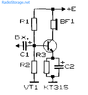
Rice. 3. A single transistor amplifier with a divider for supplying bias voltage to the base of the transistor.

Rice. 4. Single transistor amplifier with automatic bias setting for the transistor base.
In the diagram in fig. 3, the bias to the base of the transistor is set more "rigidly" with the help of a divider, which improves the quality of the amplifier when its operating conditions change. The "automatic" setting of the bias based on the amplifying transistor is used in the circuit in Fig. 4.
Two-stage transistor amplifier
By connecting in series two simplest amplification stages (Fig. 1), you can get a two-stage ULF (Fig. 5). The gain of such an amplifier is equal to the product of the gains of the individual stages. However, it is not easy to obtain a large sustained gain by subsequently increasing the number of stages: the amplifier is likely to self-excite.

Rice. 5. Scheme of a simple two-stage bass amplifier.
New developments of low-frequency amplifiers, whose circuits are often cited in the pages of magazines in recent years, are aimed at achieving a minimum total harmonic distortion, increasing output power, expanding the frequency band to be amplified, etc.
At the same time, when setting up various devices and conducting experiments, a simple ULF is often needed, which can be assembled in a few minutes. Such an amplifier should contain a minimum number of deficient elements and operate over a wide range of supply voltage and load resistance variations.
ULF circuit on field-effect and silicon transistors
A diagram of a simple LF power amplifier with direct connection between the stages is shown in Fig. 6 [Rl 3 / 00-14]. The input impedance of the amplifier is determined by the value of the potentiometer R1 and can vary from hundreds of ohms to tens of megohms. The output of the amplifier can be connected to a load with resistance from 2 ... 4 to 64 Ohm and higher.
With a high-resistance load, the KT315 transistor can be used as VT2. The amplifier is operational in the range of supply voltages from 3 to 15 V, although its acceptable performance remains even when the supply voltage is reduced to 0.6 V.
The capacitance of the C1 capacitor can be selected in the range from 1 to 100 μF. In the latter case (C1 = 100 μF), the ULF can operate in the frequency range from 50 Hz to 200 kHz and above.

Rice. 6. Scheme of a simple amplifier of low frequency on two transistors.
The amplitude of the ULF input signal should not exceed 0.5 ... 0.7 V. The output power of the amplifier can vary from tens of mW to units of W, depending on the load resistance and the magnitude of the supply voltage.
Tuning the amplifier consists in the selection of resistors R2 and R3. With their help, the voltage at the drain of the transistor VT1 is set, equal to 50 ... 60% of the voltage of the power source. Transistor VT2 must be installed on a heat sink plate (heat sink).
Direct-coupled tracked ULF
In fig. 7 shows a diagram of another seemingly simple ULF with direct connections between the stages. This kind of coupling improves the frequency response of the amplifier in the low frequency range, and the overall circuit is simplified.

Rice. 7. Schematic diagram of a three-stage ULF with direct connection between the stages.
At the same time, amplifier tuning is complicated by the fact that each amplifier impedance has to be selected individually. Roughly the ratio of resistors R2 and R3, R3 and R4, R4 and R BF should be in the range (30 ... 50) to 1. Resistor R1 should be 0.1 ... 2 kOhm. Calculation of the amplifier shown in Fig. 7 can be found in the literature, for example [P 9 / 70-60].
Cascade ULF circuits on bipolar transistors
In fig. 8 and 9 show diagrams of cascode ULF bipolar transistors. Such amplifiers have a fairly high gain Ku. The amplifier in Fig. 8 has Ku = 5 in the frequency range from 30 Hz to 120 kHz [MK 2 / 86-15]. ULF according to the scheme in Fig. 9 with a harmonic coefficient of less than 1% has a gain of 100 [RL 3 / 99-10].

Rice. 8. Cascade ULF on two transistors with gain = 5.

Rice. 9. Cascade ULF on two transistors with gain = 100.
Economical ULF on three transistors
For portable electronic equipment, an important parameter is the efficiency of the ULF. The diagram of such an ULF is shown in Fig. 10 [RL 3 / 00-14]. Here, a cascade connection of a field-effect transistor VT1 and a bipolar transistor VT3 is used, and the transistor VT2 is turned on in such a way that it stabilizes the operating point VT1 and VT3.
With an increase in the input voltage, this transistor shunts the emitter-base transition VT3 and reduces the value of the current flowing through the transistors VT1 and VT3.

Rice. 10. Scheme of a simple economical bass amplifier on three transistors.
As in the above circuit (see Fig. 6), the input impedance of this ULF can be set in the range from tens of ohms to tens of megohms. A telephone capsule was used as a load, for example, TK-67 or TM-2V. The telephone capsule, which is connected by means of a plug, can simultaneously serve as a power switch for the circuit.
The supply voltage of the ULF is from 1.5 to 15 V, although the device remains operational even when the supply voltage drops to 0.6 V. In the supply voltage range of 2 ... 15 V, the current consumed by the amplifier is described by the expression:
1 (μA) = 52 + 13 * (Upit) * (Upit),
where Usup is the supply voltage in Volts (V).
If you turn off the transistor VT2, the current consumed by the device increases by an order of magnitude.
Two-stage ULF with direct connection between stages
Examples of ULF with direct connections and a minimum selection of the operating mode are the circuits shown in Fig. 11 - 14. They have high gain and good stability.

Rice. 11. Simple two-stage ULF for a microphone (low noise, high KU).

Rice. 12. Two-stage amplifier of low frequency on transistors KT315.

Rice. 13. Two-stage low-frequency amplifier on KT315 transistors - option 2.
The microphone amplifier (Fig. 11) is characterized by a low level of intrinsic noise and high gain [MK 5/83-XIV]. An electrodynamic type microphone is used as a VM1 microphone.
A telephone capsule can also act as a microphone. Stabilization of the operating point (initial bias based on the input transistor) of the amplifiers in Fig. 11 - 13 is carried out due to the voltage drop across the emitter resistance of the second amplification stage.

Rice. 14. Two-stage ULF with a field-effect transistor.
The amplifier (Fig. 14), which has a high input impedance (about 1 MΩ), is made on a field-effect transistor VT1 (source follower) and bipolar - VT2 (with a common one).
A cascade low-frequency field-effect transistor amplifier, also having a high input impedance, is shown in Fig. 15.

Rice. 15. circuit of a simple two-stage ULF on two field-effect transistors.
ULF circuits for working with a low-ohm load
Typical ULFs designed to operate on a low-impedance load and having an output power of tens of mW and above are shown in Fig. 16, 17.

Rice. 16. Simple ULF to work with the inclusion of a load with low resistance.
The VA1 electrodynamic head can be connected to the amplifier output, as shown in Fig. 16, or in the diagonal of the bridge (Fig. 17). If the power source is made of two series-connected batteries (accumulators), the right output of the BA1 head according to the scheme can be connected directly to their midpoint, without capacitors СЗ, С4.
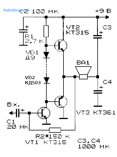
Rice. 17. Low-frequency amplifier circuit with the inclusion of a low-impedance load in the diagonal of the bridge.
If you need a circuit of a simple tube ULF, then such an amplifier can be assembled even on one lamp, look at our electronics website in the appropriate section.
Literature: Shustov M.A. Practical Circuitry (Book 1), 2003.
Corrections in the publication: in fig. 16 and 17, instead of diode D9, a chain of diodes is installed.