![]() First transistor
First transistor
In the photo on the right you see the first working transistor, which was created in 1947 by three scientists - Walter Brattain, John Bardeen and William Shockley.
Despite the fact that the first transistor did not have a very presentable appearance, this did not prevent him from revolutionizing radio electronics.
It is difficult to imagine what the current civilization would be like if the transistor had not been invented.
The transistor is the first solid state device capable of amplifying, generating and converting an electrical signal. It has no vibration-prone parts and is compact in size. This makes it very attractive for electronic applications.
It was a small introduction, and now let's take a closer look at what a transistor is.
First, it is worth recalling that transistors are divided into two large classes. The first includes the so-called bipolar, and the second - field (they are also unipolar). The basis of both field and bipolar transistors is a semiconductor. The main material for the production of semiconductors is germanium and silicon, as well as a compound of gallium and arsenic - gallium arsenide ( GaAs).
It is worth noting that silicon-based transistors are the most widely used, although this fact may soon be shaken, as technology develops continuously.
It just so happened, but at the beginning of the development of semiconductor technology, the bipolar transistor took the leading place. But not many people know that initially the focus was on the creation of a field-effect transistor. He was brought to mind later. Read about MOSFETs.
We will not go into a detailed description of the device of the transistor at the physical level, but first we will find out how it is indicated on the circuit diagrams. For beginners in electronics, this is very important.
To begin with, it must be said that bipolar transistors can be of two different structures. It's a P-N-P and N-P-N structure. While not getting into theory, just remember that a bipolar transistor can be either P-N-P or N-P-N.
On circuit diagrams, bipolar transistors are designated like this.

As you can see, the figure shows two conditional graphic symbols. If the arrow inside the circle is directed towards the central line, then this is a transistor with a P-N-P structure. If the arrow is directed outward, then it has the N-P-N structure.
Little advice.
In order not to remember the symbol, and immediately determine the type of conductivity (p-n-p or n-p-n) of a bipolar transistor, you can use this analogy.
First, let's look at where the arrow points on the conditional image. Next, we imagine that we are going in the direction of the arrow, and if we run into the “wall” - a vertical line - then, then, “Pass H em! " H et" means p- n-p (P- H-P ).
Well, if we go, and do not rest against the "wall", then the diagram shows an n-p-n structure transistor. A similar analogy can be used with field effect transistors when determining the type of channel (n or p). Read about the designation of different field-effect transistors in the diagram
Usually, discrete, that is, a separate transistor has three outputs. Previously, it was even called a semiconductor triode. Sometimes it may have four leads, but the fourth is used to connect the metal case to a common wire. It is shielding and is not connected to other pins. Also, one of the conclusions, usually a collector (it will be discussed later), may be in the form of a flange for attaching to a cooling radiator or be part of a metal case.
Here take a look. The photo shows various transistors from the Soviet production, as well as the early 90s.

But this is a modern import.

Each of the outputs of the transistor has its own purpose and name: base, emitter and collector. Usually these names are abbreviated and written simply B ( Base), E ( emitter), TO ( Collector). On foreign circuits, the collector output is marked with the letter C, this is from the word Collector- "collector" (verb Collect- "collect"). Base output is marked as B, from the word Base(from the English. Base - "main"). This is the control electrode. Well, the output of the emitter is denoted by the letter E, from the word Emitter- "emitter" or "source of emissions". In this case, the emitter serves as a source of electrons, so to speak, as a supplier.
![]()
The outputs of the transistors must be soldered into the electronic circuit, strictly observing the pinout. That is, the collector output is soldered exactly in that part of the circuit where it should be connected. It is impossible to solder the output of the collector or emitter instead of the base output. Otherwise, the circuit will not work.
How to find out where in the circuit diagram the collector is, and where is the emitter? Everything is simple. The one with the arrow is always the emitter. The one that is drawn perpendicular (at an angle of 90 0) to the central line is the output of the base. And the one that remains is the collector.
Also on the circuit diagrams, the transistor is marked with the symbol VT or Q. In old Soviet books on electronics, you can find a designation in the form of a letter V or T. Next, the serial number of the transistor in the circuit is indicated, for example, Q505 or VT33. It should be borne in mind that the letters VT and Q denote not only bipolar transistors, but also field ones.
In real electronics, transistors are easily confused with other electronic components, such as triacs, thyristors, integrated regulators, since they have the same package. It is especially easy to get confused when an unknown marking is applied to an electronic component.
In this case, you need to know that positioning is marked on many printed circuit boards and the type of element is indicated. This is the so-called silkscreen. So on the printed circuit board next to the part, Q305 can be written. This means that this element is a transistor and its serial number in the circuit diagram is 305. It also happens that the name of the transistor electrode is indicated next to the terminals. So, if there is a letter E next to the output, then this is the emitter electrode of the transistor. Thus, it is possible to determine purely visually what is installed on the board - a transistor or a completely different element.
As already mentioned, this statement is true not only for bipolar transistors, but also for field ones. Therefore, after determining the type of element, it is necessary to specify the class of the transistor (bipolar or field) according to the marking applied to its case.

Field effect transistor FR5305 on the printed circuit board of the device. The element type is indicated next to it - VT
Any transistor has its own rating or marking. Marking example: KT814. From it you can find out all the parameters of the element. As a rule, they are indicated in the datasheet (datasheet). It is also a reference sheet or technical documentation. There may also be transistors of the same series, but with slightly different electrical parameters. Then the name contains additional characters at the end, or, more rarely, at the beginning of the marking. (for example, the letter A or D).
Why bother with all sorts of additional designations? The fact is that in the manufacturing process it is very difficult to achieve the same characteristics for all transistors. There is always a certain, albeit small, but difference in the parameters. Therefore, they are divided into groups (or modifications).
Strictly speaking, the parameters of transistors of different batches can vary quite significantly. This was especially noticeable earlier, when the technology of their mass production was only being perfected.
Popular science edition
Yatsenkov Valery Stanislavovich
Secrets of foreign radio circuits
Tutorial-reference book for the master and amateur
Editor A.I. Osipenko
Proofreader V.I. Kiseleva
Computer layout by A. S. Varakina
B.C. Yatsenkov
SECRETS
FOREIGN
RADIO SCHEMES
Reference textbook
for the master and amateur
Moscow
Major Publisher Osipenko A.I.
2004
Secrets of foreign radio circuits. Tutorial reference for
master and amateur. - M.: Mayor, 2004. - 112 p.
From the author
1. Main types of schemes 1.1. Functional diagrams 1.2. Schematic diagrams 1.3. Illustrative images 2. Conditional graphic designations of elements of circuit diagrams 2.1. Conductors 2.2. Switches, connectors 2.3. Electromagnetic relays 2.4. Sources of electrical energy 2.5. Resistors 2.6. Capacitors 2.7. Coils and transformers 2.8. Diodes 2.9. Transistors 2.10. Dinistors, thyristors, triacs 2.11. Vacuum electron tubes 2.12. Discharge lamps 2.13. Incandescent lamps and signal lamps 2.14. Microphones, sound emitters 2.15. Fuses and circuit breakers 3. Independent application of circuit diagrams step by step 3.1. Construction and analysis of a simple circuit 3.2. Analysis of a complex circuit 3.3. Assembly and debugging of electronic devices 3.4. Repair of electronic devices
The author refutes the common misconception that the reading of radio circuits and their use in the repair of household equipment is available only to trained professionals. A large number of illustrations and examples, a lively and accessible language of presentation make the book useful for readers with an initial level of knowledge of radio engineering. Particular attention is paid to the designations and terms used in foreign literature and documentation for imported household appliances.
FROM THE AUTHOR
First of all, dear reader, we thank you for your interest in this book.
The brochure that you are holding in your hands is only the first step on the path to incredibly fascinating knowledge. The author and publisher will consider their task accomplished if this book not only serves as a reference for beginners, but also gives them confidence in their abilities.
We will try to clearly show that for self-assembly of a simple electronic circuit or a simple repair of a household appliance, you do not need to have big amount of specialized knowledge. Of course, to develop your own circuit, you will need knowledge of circuitry, that is, the ability to build a circuit in accordance with the laws of physics and in accordance with the parameters and purpose of electronic devices. But even in this case, one cannot do without a graphic language of diagrams in order to first correctly understand the material of the textbooks, and then correctly state one's own thought.
Preparing the publication, we did not set ourselves the goal of retelling in a concise form the content of GOSTs and technical standards. First of all, we appeal to those readers for whom an attempt to put into practice or independently depict an electronic circuit causes confusion. Therefore, the book covers only most commonly used symbols and designations, without which no scheme can do. Further reading skills and drawing circuit diagrams will come to the reader gradually, as he gains practical experience. In this sense, learning the language of electronic circuits is similar to learning a foreign language: first we memorize the alphabet, then the simplest words and the rules by which a sentence is built. Further knowledge comes only with intensive practice.
One of the problems faced by novice radio amateurs who are trying to repeat the scheme of a foreign author or repair a household device is that there is a discrepancy between the system of conventional graphic symbols (UGO) adopted earlier in the USSR and the UGO system operating in foreign countries. Due to the wide distribution of design programs equipped with UGO libraries (almost all of them were developed abroad), foreign circuit designations also invaded domestic practice, despite the GOST system. And if an experienced specialist is able to understand the meaning of an unfamiliar symbol, based on the general context of the scheme, then this can cause serious difficulties for a novice amateur.
In addition, the language of electronic circuits periodically undergoes changes and additions, the style of some symbols changes. In this book, we will mainly rely on the international notation system, since it is it that is used in diagrams for imported household equipment, in standard symbol libraries for popular computer programs, and on pages of foreign websites. Notations will also be mentioned that are officially obsolete, but in practice are found in many schemes.
1. MAIN TYPES OF SCHEMES
In radio engineering, three main types of circuits are most often used: functional diagrams, electrical circuit diagrams and visual images. When studying the circuit of any electronic device, as a rule, all three types of circuits are used, and in the order listed. In some cases, to improve clarity and convenience, schemes can be partially combined.
Functional diagram gives a visual representation of the overall structure of the device. Each functionally completed node is represented on the diagram as a separate block (rectangle, circle, etc.), indicating the function it performs. The blocks are connected to each other by lines - solid or dashed, with or without arrows, in accordance with how they affect each other in the process of work.
Circuit diagram shows which components are included in the circuit and how they are connected to each other. The circuit diagram often indicates the waveforms of the signals and the magnitude of the voltage and current at the control points. This kind of schemes is the most informative, and we will pay the most attention to it.
illustrative images exist in several versions and are intended, as a rule, to facilitate installation and repair. These include layouts of elements on a printed circuit board; schemes for laying connecting conductors; schemes for connecting individual nodes to each other; layouts of nodes in the product case, etc.
1.1. FUNCTIONAL DIAGRAM
Rice. 1-1. Functional Diagram Examplecomplex of finished devices
Functional diagrams can be used for several different purposes. Sometimes they are used to show how various functionally complete devices interact with each other. An example is the connection diagram of a television antenna, a VCR, a TV and an infrared remote control that controls them (Fig. 1-1). A similar scheme can be seen in any instruction manual for a VCR. Looking at this diagram, we understand that the antenna must be connected to the VCR input in order to be able to record programs, and the remote control is universal and can control both devices. Note that the antenna is shown with a symbol that is also used in circuit diagrams. Such a "mixing" of symbols is allowed in the case when a functionally completed assembly is a part that has its own graphic designation. Looking ahead, let's say that reverse situations also occur, when a part of a circuit diagram is depicted as a functional block.
If, when constructing a block diagram, priority is given to the image of the structure of a device or a complex of devices, such a diagram is called structural. If the block diagram is an image of several nodes, each of which performs a specific function, and the links between the blocks are shown, then such a diagram is usually called functional. This division is to some extent conditional. For example, fig. 1-1 simultaneously shows both the structure of the home video complex and the functions performed by individual devices, and the functional relationships between them.
When constructing functional circuits, it is customary to follow certain rules. The main one is that the direction of the signal (or the order of execution of functions) is displayed on the drawing from left to right and from top to bottom. Exceptions are made only when the circuit has complex or bidirectional functional relationships. Permanent connections through which signals propagate are made with solid lines, if necessary - with arrows. Non-permanent connections, acting depending on some condition, are sometimes shown with dotted lines. When developing a functional diagram, it is important to choose the right level of detail. For example, you should consider whether to depict the pre-amplifier and final amplifier in the diagram as different blocks, or as one? It is desirable that the level of detail is the same for all circuit components.
As an example, consider the circuit of a radio transmitter with an amplitude modulated output signal in Fig. 1-2a. It consists of a low frequency part and a high frequency part.

Rice. 1-2a. Functional diagram of a simple AM transmitter
We are interested in the direction of transmission of the speech signal, we take its direction as a priority, and draw the low-frequency blocks at the top, from where the modulating signal, passing from left to right through the low-frequency blocks, falls down into the high-frequency blocks.
The main advantage of functional circuits is that, under the condition of optimal detailing, universal circuits are obtained. Different radio transmitters may use completely different circuit diagrams of the master oscillator, modulator, etc., but the circuits with a low degree of detail will be exactly the same.
Another thing is if deep detailing is applied. For example, in one radio transmitter, the reference frequency source has a transistor multiplier, in another, a frequency synthesizer is used, and in the third, a simple quartz oscillator. Then the detailed functional diagrams for these transmitters will be different. Thus, some nodes on the functional diagram, in turn, can also be represented in the form of a functional diagram.
Sometimes, in order to focus on a particular feature of the circuit or increase its clarity, combined circuits are used (Fig. 1-26 and 1-2c), in which the image of functional blocks is combined with a more or less detailed fragment of a circuit diagram.
Rice. 1-2b. Combined Circuit Example

Rice. 1-2c. Combined Circuit Example
The block diagram shown in fig. 1-2a is a kind of functional diagram. It does not show exactly how and how many conductors the blocks are connected to each other. For this purpose it serves wiring diagram(Fig. 1-3).
Rice. 1-3. Interconnect Diagram Example
Sometimes, especially when it comes to devices on logic chips or other devices that operate according to a certain algorithm, it is necessary to schematically depict this algorithm. Of course, the operation algorithm does not reflect the features of the construction of the electrical circuit of the device, but it can be very useful when repairing or configuring it. When depicting an algorithm, they usually use standard symbols used in documenting programs. On fig. 1-4 show the most commonly used characters.
As a rule, they are sufficient to describe the operation algorithm of an electronic or electromechanical device.
As an example, consider a fragment of the algorithm for the operation of the automation unit of a washing machine (Fig. 1-5). After turning on the power, the presence of water in the tank is checked. If the tank is empty, the inlet valve opens. The valve is then held open until the high level sensor is triggered.
Beginning or end of the algorithm

An arithmetic operation performed by a program, or some action performed by a device
Comment, explanation or description

Input or output operation
Library module of the program

Jump by condition
Unconditional jump
Page transition
Connecting lines
Rice. 1-4. Basic symbols for describing algorithms

Rice. 1-5. An example of the operation algorithm of the automation unit
1.2. PRINCIPAL
ELECTRICAL CIRCUITS
Quite a long time ago, at the time of Popov's first radio receiver, there was no clear distinction between visual and circuit diagrams. The simplest devices of that time were quite successfully depicted in the form of a slightly abstracted picture. And now in textbooks you can find an image of the simplest electrical circuits in the form of drawings, in which the details are shown approximately as they actually look and how their conclusions are interconnected (Fig. 1-6).

Rice. 1-6. Example of difference between wiring diagram (A)
and circuit diagram (B).
But for a clear understanding of what a circuit diagram is, you should remember: the placement of symbols on the circuit diagram does not necessarily correspond to the actual placement of the components and connecting conductors of the device. Moreover, a common mistake novice hams make when designing a printed circuit board on their own is to try to place the components as close as possible to the order in which they are shown on the circuit diagram. As a rule, the optimal placement of components on the board is significantly different from the placement of symbols on the circuit diagram.
So, on the circuit diagram, we see only conventional graphic designations of the elements of the device circuit with an indication of their key parameters (capacitance, inductance, etc.). Each component of the circuit is numbered in a certain way. In the national standards of different countries regarding the numbering of elements, there are even greater differences than in the case of graphic symbols. Since we set ourselves the task of teaching the reader to understand the circuits depicted according to "Western" standards, we will give a short list of the main letter designations of the components:
| Letter designation | Meaning | Meaning |
| ANT | Antenna | Antenna |
| IN | Battery | Battery |
| FROM | Capacitor | Capacitor |
| SW | circuit board | Circuit board |
| CR | Zener Diode | zener diode |
| D | diode | Diode |
| EP or Earphone | RN | Headphones |
| F | fuse | Fuse |
| I | Lamp | incandescent lamp |
| IC | Integrated circuit | Integrated circuit |
| J | Receptacle, Jack, Terminal Strip | Socket, cartridge, terminal block |
| TO | Relay | Relay |
| L | Inductor, choke | Coil, choke |
| LED | Light emitting diode | Light-emitting diode |
| M | meter | Meter (generalized) |
| N | neon lamp | Neon lamp |
| R | Plug | Plug |
| PC | Photocell | Photocell |
| Q | Transistor | Transistor |
| R | resistor | Resistor |
| RFC | radio frequency choke | High frequency choke |
| R.Y. | Relay | Relay |
| S | switch | switch, switch |
| SPK | speaker | Speaker |
| T | transformer | Transformer |
| U | Integrated circuit | Integrated circuit |
| V | vacuum tube | radio tube |
| VR | voltage regulator | Regulator (stabilizer) e.g. |
| X | solar cells | solar cell |
| XTAL or Crystal | Quartz resonator Y | |
| Z | circuit assembly | Schematic Assembly Assembly |
| ZD | Zener Diode (rare) | Zener diode (obsolete) |
Many circuit components (resistors, capacitors, etc.) may appear more than once in the drawing, so a digital index is added to the letter designation. For example, if there are three resistors in the circuit, they will be labeled as R1, R2 and R3.
Schematic diagrams, like block diagrams, are arranged in such a way that the input of the circuit is on the left and the output is on the right. An input signal also means a power source if the circuit is a converter or regulator, and an output means a power consumer, an indicator or an output stage with output terminals. For example, if we draw a diagram of a flash lamp, then we draw a mains plug, a transformer, a rectifier, a pulse generator and a flash lamp in order from left to right.
Elements are numbered from left to right and top to bottom. In this case, the possible placement of elements on the printed circuit board has nothing to do with the numbering order - the circuit diagram has the highest priority in relation to other types of circuits. An exception is made when, for greater clarity, the circuit diagram is divided into blocks corresponding to the functional diagram. Then a prefix is added to the element designation, corresponding to the block number on the functional diagram: 1-R1, 1-R2, 2L1, 2L2, etc.
In addition to the alphanumeric index, next to the graphic designation of the element, its type, brand or denomination is often written, which are of fundamental importance for the operation of the circuit. For example, for a resistor this is the resistance value, for a coil it is inductance, for a microcircuit it is the manufacturer's marking. Sometimes information about the ratings and markings of components is taken out in a separate table. This method is convenient in that it allows you to give extended information about each component - coil winding data, special requirements for the type of capacitors, etc.
1.3. VISUAL IMAGES
Schematic diagrams and functional block diagrams complement each other well and are easy to understand with minimal experience. However, very often these two schemes are not enough to fully understand the design of the device, especially when it comes to repairing or assembling it. In this case, several types of visual images are used.
We already know that circuit diagrams do not show the physical essence of the installation, and visual images solve this problem. But, unlike block diagrams, which can be the same for different electrical circuits, visual images are inseparable from their corresponding circuit diagrams.
Let's look at a few visual examples. On fig. 1-7 shows a type of wiring diagram - a wiring diagram of the connecting conductors assembled into a shielded bundle, and the pattern most closely matches the laying of conductors in a real device. Note that sometimes, to facilitate the transition from a circuit diagram to a wiring diagram, the circuit diagram also indicates the color marking of the conductors and the shielded wire symbol.

Rice. 1-7. Example of wiring diagram for connecting conductors
The next widely used type of visual images are various layouts of elements. Sometimes they are combined with the wiring diagram. The scheme shown in fig. 1-8 gives us enough information about the components that the microphone amplifier circuit should consist of so that we can purchase them, but does not tell us anything about the physical dimensions of the components, the board and the case, or the placement of the components on the board. But in many cases, the placement of components on the board and/or in the package is critical to the reliable operation of the device.
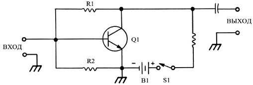
Rice. 1-8. Diagram of a simple microphone amplifier
The previous diagram is successfully supplemented by the wiring diagram fig. 1-9. This is a two-dimensional diagram, it can indicate the length and width of the case or board, but not the height. If it is necessary to indicate the height, then a side view is given separately. Components are depicted as symbols, but their icons have nothing to do with UGOs, but are closely related to the actual appearance of the part. Of course, the addition of such a simple circuit diagram with a wiring diagram may seem superfluous, but this cannot be said about more complex devices consisting of tens and hundreds of parts.
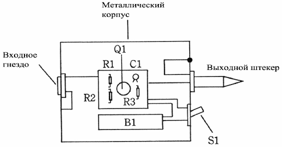
Rice. 1-9. Visual illustration of the installation for the previous circuit
The most important and most common type of wiring diagrams is layout of elements on a printed circuit board. The purpose of such a diagram is to indicate the order of placement of electronic components on the board during installation and to facilitate their location during repair (recall that the placement of components on the board does not correspond to their location on the circuit diagram). One of the options for a visual representation of the printed circuit board is shown in Fig. 1-10. In this case, although conditionally, the shape and dimensions of all components are shown quite accurately, and their symbols are numbered, coinciding with the numbering on the circuit diagram. Dashed outlines show elements that may not be present on the board.

Rice. 1-10. PCB image option
This option is convenient for repairs, especially when a specialist works, who knows from his own experience the characteristic appearance and dimensions of almost all radio components. If the circuit consists of many small and similar elements, and for repair it is required to find many control points on the board (for example, to connect an oscilloscope), then the work becomes much more complicated even for a specialist. In this case, the coordinate layout of the elements comes to the rescue (Fig. 1-1 1).

Rice. 1-11. Coordinate layout of elements
The applied coordinate system is somewhat reminiscent of coordinates on a chessboard. In this example, the board is divided into two, marked with the letters A and B, longitudinal parts (there may be more) and transverse parts with numbers. Board image added element placement table, an example of which is given below:
| Ref design | Grid Loc | Ref design | Grid Loc | Ref design | Grid Loc | Ref design | Grid Loc | Ref design | Grid Loc |
| C1 | B2 | C45 | A6 | Q10 | R34 | A3 | R78 | B7 | |
| C2 | B2 | C46 | A6 | Q11 | R35 | A4 | R79 | B7 | |
| C3 | B2 | C47 | A7 | Q12 | B5 | R36 | A4 | R80 | B7 |
| C4 | B2 | C48 | B7 | Q13 | R37 | A4 | R81 | B8 | |
| C5 | B3 | C49 | A7 | Q14 | A8 | R38 | B4 | R82 | B7 |
| C6 | B3 | C50 | A7 | Q15 | A8 | R39 | A4 | R83 | B7 |
| C7 | B3 | C51 | A7 | Q16 | B5 | R40 | A4 | R84 | B7 |
| C8 | B3 | C52 | A8 | Q17 | R41 | R85 | B7 | ||
| C9 | B3 | C53 | 018 | R42 | R86 | B7 | |||
| C10 | B3 | C54 | Q19 | B8 | R43 | B3 | R87 | Al | |
| C11 | B4 | C54 | A4 | Q20 | A8 | R44 | A4 | R88 | A6 |
| C12 | B4 | C56 | A4 | Rl | B2 | R45 | A4 | R89 | B6 |
| C13 | B3 | C57 | B6 | R2 | B2 | R46 | A4 | R90 | B6 |
| C14 | B4 | C58 | B6 | R3 | B2 | K47 | R91 | A6 | |
| C15 | A2 | CR1 | VZ | R4 | VZ | R48 | R92 | A6 | |
| C16 | A2 | CR2 | B3 | R5 | VZ | R49 | AT 5 | R93 | A6 |
| C17 | A2 | CR3 | B4 | R6 | AT 4 | R50 | R94 | A6 | |
| C18 | A2 | CR4 | R7 | AT 4 | R51 | AT 5 | R93 | A6 | |
| C19 | A2 | CR5 | A2 | R8 | AT 4 | R52 | AT 5 | R94 | A6 |
| C20 | A2 | CR6 | A2 | R9 | AT 4 | R53 | A3 | R97 | A6 |
| C21 | A3 | CR7 | A2 | R10 | AT 4 | R54 | A3 | R98 | A6 |
| C22 | A3 | CR8 | A2 | R11 | AT 4 | R55 | A3 | R99 | A6 |
| C23 | A3 | CR9 | RI2 | R56 | A3 | R101 | A7 | ||
| C24 | B3 | CR10 | A2 | RI3 | R57 | VZ | R111 | A7 | |
| C25 | A3 | CR11 | A4 | RI4 | A2 | R58 | VZ | R112 | A6 |
| C26 | A3 | CR12 | A4 | RI5 | A2 | R39 | VZ | R113 | A7 |
| C27 | A4 | CR13 | AT 8 | R16 | A2 | R60 | B5 | R104 | A7 |
| C28 | AT 6 | CR14 | A6 | R17 | A2 | R61 | AT 5 | R105 | A7 |
| C29 | IN 3 | CR15 | A6 | R18 | A2 | R62 | R106 | A7 | |
| C30 | CR16 | A7 | R19 | A3 | R63 | AT 6 | R107 | A7 | |
| C31 | AT 5 | L1 | IN 2 | R20 | A2 | R64 | AT 6 | R108 | A7 |
| C32 | AT 5 | L2 | IN 2 | R21 | A2 | R65 | AT 6 | R109 | A7 |
| SPZ | A3 | L3 | VZ | R22 | A2 | R66 | AT 6 | R110 | A7 |
| C34 | A3 | L4 | VZ | R23 | A4 | R67 | AT 6 | U1 | A1 |
| C35 | AT 6 | L5 | A3 | R24 | A3 | R6S | AT 6 | U2 | A5 |
| C36 | AT 7 | Q1 | VZ | R2S | A3 | R69 | AT 6 | U3 | AT 6 |
| C37 | AT 7 | Q2 | AT 4 | R26 | A3 | R7U | AT 6 | U4 | AT 7 |
| C38 | AT 7 | Q3 | Q4 | R27 | IN 2 | R71 | AT 6 | U5 | A6 |
| C39 | AT 7 | Q4 | R28 | A2 | R72 | AT 7 | U6 | A7 | |
| C40 | AT 7 | Q5 | IN 2 | R29 | R73 | AT 7 | |||
| C41 | AT 7 | Q6 | A2 | R30 | R74 | AT 7 | |||
| C42 | AT 7 | O7 | A3 | R31 | VZ | R75 | AT 7 | ||
| C43 | AT 7 | Q8 | A3 | R32 | A3 | R76 | AT 7 | ||
| C44 | AT 7 | Q9 | A3 | R33 | A3 | R77 | AT 7 |
When designing a printed circuit board using one of the design programs, the element placement table can be generated automatically. The use of a table greatly facilitates the search for elements and control points, but increases the volume of design documentation.
In the manufacture of printed circuit boards in the factory, they are often marked with designations similar to Fig. 1-10 or fig. 1-11. It is also a kind of visual representation of the montage. It can be supplemented with the physical contours of the elements, to facilitate the installation of the circuit (Fig. 1-12). 
Rice. 1-12. Drawing of PCB conductors.
It should be noted that the development of a printed circuit board design begins with the placement of elements on a board of a given size. When placing the elements, their shape and dimensions, the possibility of mutual influence, the need for ventilation or shielding, etc. are taken into account. Then the connecting conductors are routed, if necessary, the placement of the elements is corrected and the final wiring is performed.
2. SYMBOLS
As we already mentioned in Chapter 1, the graphical symbols (UGO) of radio-electronic components used in modern circuitry have a rather remote relation to the physical essence of a particular radio component. An example is the analogy between a circuit diagram of a device and a map of a city. On the map, we see an icon indicating a restaurant, and we understand how to get to the restaurant. But this icon does not say anything about the restaurant menu and prices for ready meals. In turn, the graphic symbol that denotes a transistor on the diagram does not say anything about the size of the case of this transistor, whether its conclusions are flexible, and which company manufactured it.
On the other hand, on the map, next to the designation of the restaurant, the schedule of its work can be indicated. Similarly, near the UGO components in the diagram, important technical parameters of the part are usually indicated, which are of fundamental importance for the correct understanding of the circuit. For resistors, this is resistance, for capacitors, it is capacitance, for transistors and microcircuits, it is an alphanumeric designation, etc.
Since its inception, UGO electronic components have undergone significant changes and additions. At first, these were rather naturalistic drawings of details, which then, over time, were simplified and abstracted. However, to make it easier to work with symbols, most of them still carry some hint of the design features of the real part. Talking about graphic symbols, we will try to show this relationship as far as possible.
Despite the apparent complexity of many circuit diagrams, understanding them requires little more work than understanding a road map. There are two different approaches to acquiring the skill of reading circuit diagrams. Proponents of the first approach believe that UGO is a kind of alphabet, and you should first memorize it as fully as possible, and then start working with diagrams. Supporters of the second method believe that it is necessary to start reading diagrams almost immediately, studying unfamiliar characters along the way. The second method is good for a radio amateur, but, alas, it does not accustom to a certain rigor of thinking necessary for the correct image of circuits. As you will see below, the same diagram can be depicted in completely different ways, and some of the options are extremely unreadable. Sooner or later, there will be a need to draw your own scheme, and this should be done in such a way that it is clear at first sight not only to the author. We give the reader the right to decide for himself which approach is closer to him, and proceed to the study of the most common graphic symbols.
2.1. CONDUCTORS
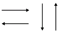
Most circuits contain a significant number of conductors. Therefore, the lines depicting these conductors often intersect in the diagram, while there is no contact between the physical conductors. Sometimes, on the contrary, it is necessary to show the connection of several conductors to each other. On fig. 2-1 shows three options for crossing conductors.

Rice. 2-1. Variants of the image of the intersection of conductors
Option (A) denotes the connection of crossing conductors. In case (B) and (C) the conductors are not connected, but the designation (C) is considered obsolete and should be avoided in practice. Of course, the intersection of mutually insulated conductors in a circuit diagram does not mean their constructive intersection.
Several conductors can be combined into a bundle or cable. If the cable does not have a braid (screen), then, as a rule, these conductors are not particularly distinguished in the diagram. There are special symbols for shielded wires and cables (fig. 2-2 and 2-3). An example of a shielded conductor is a coaxial antenna cable.

Rice. 2-2. Single shielded conductor symbols with ungrounded (A) and grounded (B) shield

Rice. 2-3. Shielded cable symbols with ungrounded (A) and grounded (B) shield
Sometimes the connection must be made with a twisted pair of conductors.
Rice. 2-4. Two options for designating twisted-pair wires
In Figures 2-2 and 2-3, in addition to conductors, we see two new graphical elements that will be encountered further. The dotted closed contour denotes a screen, which can be structurally made in the form of a braid around the conductor, in the form of a closed metal case, a separating metal plate or a grid.
The screen prevents the penetration of interference into circuits that are sensitive to external pickups. The next symbol is an icon indicating a connection to common, ground, or ground. In circuitry, several symbols are used for this.
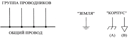
Rice. 2-5. Designations of a common wire and various groundings
The term "grounding" has a long history and dates back to the days of the first telegraph lines, when the Earth was used as one of the conductors to save wires. At the same time, all telegraph devices, regardless of their connection to each other, were connected to the Earth using grounding. In other words, the earth was common wire. In modern circuitry, the term "ground" (ground) refers to a common wire or a wire with zero potential, even if it is not connected to a classic ground (Fig. 2-5). The common wire can be insulated from the body of the device.
Very often, the body of the device is used as a common wire, or the common wire is electrically connected to the body. In this case, the icons (A) and (B) are used. Why are they different? There are circuits that combine analog components, such as operational amplifiers and digital ICs. To avoid mutual interference, especially from digital to analog circuits, use a separate common wire for analog and digital circuits. In everyday life, they are called "analog ground" and "digital ground". Similarly, shared wires for low-current (signal) and power circuits.
2.2. SWITCHES, CONNECTORS
A switch is a device, mechanical or electronic, that allows you to change or break an existing connection. The switch allows, for example, to send a signal to any element of the circuit or to bypass this element (Fig. 2-6).

Rice. 2-6. Breakers and switches
A special case of a switch is a switch. On fig. 2-6 (A) and (B) show single and double switches, and fig. 2-6 (C) and (D) single and double switches, respectively. These switches are called on-off, since they have only two stable positions. As you can easily see, the symbols of the switch and the switch depict the corresponding mechanical structures in sufficient detail and have not changed much since their inception. Currently, this design is used only in power electrical circuit breakers. Used in low voltage electronic circuits toggle switches And sliding switches. For toggle switches, the designation remains the same (Fig. 2-7), and for sliding switches, a special designation is sometimes used (Fig. 2-8).
The switch is usually depicted in the diagram in off state, unless specifically stated the need to depict it included.
It is often required to use multi-position switches that allow switching a large number of signal sources. They can also be single or double. The most convenient and compact design have rotary multiposition switches(Figure 2-9). Such a switch is often referred to as a "biscuit" switch, because when switched it makes a sound similar to the crunch of a dry biscuit being broken. The dotted line between the individual symbols (groups) of the switch means a rigid mechanical connection between them. If, due to the nature of the scheme, switching groups cannot be placed side by side, then an additional group index is used to designate them, for example, S1.1, S1.2, S1.3. In this example, three mechanically connected groups of one switch S1 are designated in this way. When depicting such a switch in the diagram, it is necessary to ensure that all groups have the switch slider set to the same position.

Rice. 2-7. Symbols for different options for toggle switches
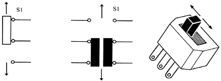
Rice. 2-8. Sliding switch symbol

Rice. 2-9. Multi-position rotary switches
The next group of mechanical switches are pushbutton switches and switches. These devices differ in that they do not work by shifting or turning, but by pressing.
On fig. 2-10 shows the symbols of push-button switches. There are buttons with normally open contacts, normally closed, single and double, as well as switching single and double. There is a separate, although rarely used, designation for the telegraph key (manual formation of Morse code), shown in Fig. 2-11.

Rice. 2-10. Various pushbutton options

Rice. 2-11. Special telegraph key symbol
Connectors are used for non-permanent connection to the circuit of external connecting conductors or components (Figure 2-12).

 Rice. 2-12. Common connector designations
Connectors are divided into two main groups: sockets and plugs. Exceptions are some types of pressure connectors, such as charger contacts for the handset of a radiotelephone.
But even in this case, they are usually depicted as a socket (charger) and a plug (a phone handset inserted into it).
On fig. Figure 2-12(A) shows symbols for Western standard sockets and plugs. Symbols with filled rectangles indicate plugs, to the left of them - the symbols of the corresponding sockets.
Further on fig. 2-12 shows: (B) - an audio jack for connecting headphones, a microphone, low-power speakers, etc.; (C) - a "tulip" connector, usually used in video equipment for connecting cables of audio and video channels; (D) - connector for connecting a high-frequency coaxial cable. A filled circle in the center of the symbol indicates a plug, while an open circle indicates a socket.
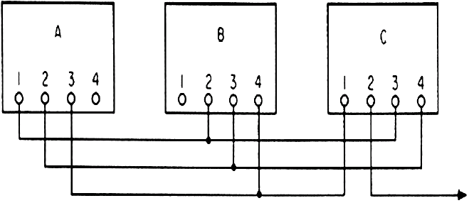
Connectors can be combined into contact groups when it comes to a multi-pin connector. In this case, the symbols of single contacts are graphically combined using a solid or dashed line.
2.3. ELECTROMAGNETIC RELAYS
Electromagnetic relays can also be attributed to the group of switches. But, unlike buttons or toggle switches, in a relay, the contacts switch under the influence of the force of attraction of an electromagnet.
If the contacts are closed when the winding is de-energized, they are called normally closed, otherwise - normally open.
There are also switching contacts.
The diagrams, as a rule, show the position of the contacts with a de-energized winding, unless this is specifically mentioned in the description of the circuit.
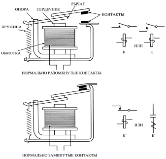
Rice. 2-13. The design of the relay and its symbol
The relay can have several contact groups acting synchronously (Fig. 2-14). In complex circuits, the relay contacts may be shown separately from the winding symbol. The relay in the complex or its winding is indicated by the letter K, and to designate the contact groups of this relay, a digital index is added to the alphanumeric designation. For example, K2.1 designates the first contact group of relay K2.

Rice. 2-14. Relays with one and several contact groups
In modern foreign circuits, the relay winding is increasingly denoted as a rectangle with two leads, as has long been accepted in domestic practice.
In addition to conventional electromagnetic relays, polarized relays are sometimes used, the distinguishing feature of which is that the armature switches from one position to another when the polarity of the voltage applied to the winding changes. In the disconnected state, the armature of the polarized relay remains in the position it was in before the power was turned off. Currently, polarized relays are practically not used in common circuits.
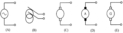
2.4. SOURCES OF ELECTRIC ENERGY
Sources of electrical energy are divided into primary: generators, solar cells, chemical sources; And secondary: converters and rectifiers. Both those and others can either be depicted on the circuit diagram, or not. It depends on the features and purpose of the scheme. For example, in the simplest circuits, very often, instead of a power source, only connectors for connecting it are shown, indicating the rated voltage, and sometimes the current consumed by the circuit. Indeed, for a simple amateur radio design, it does not really matter whether it will be powered by a Krona battery or a laboratory rectifier. On the other hand, a household appliance usually includes a built-in mains power supply, and it will necessarily be shown in the form of an expanded diagram in order to facilitate maintenance and repair of the product. But this will be a secondary source of power supply, since we would have to specify a hydroelectric generator and intermediate transformer substations as a primary source, which would be quite meaningless. Therefore, on the diagrams of devices powered by public power networks, they are limited to the image of the mains plug.
On the contrary, if the generator is an integral part of the design, it is depicted in a circuit diagram. As an example, we can cite the schemes of the on-board network of a car or an autonomous generator driven by an internal combustion engine. There are several common generator symbols (Figure 2-15). Let us comment on these notations.
(A) is the most common symbol for an alternator.
(B) - used when it is necessary to indicate that the voltage is removed from the generator winding using spring contacts (brushes) pressed against ring rotor outlets. Such alternators are usually used in automobiles.
(C) - a generalized symbol of the design, in which the brushes are pressed against the segmented terminals of the rotor (collector), i.e., to the contacts in the form of metal pads located around the circumference. This symbol is also used to designate electric motors of a similar design.
(D) - the filled elements of the symbol indicate that brushes made of graphite are used. The letter A indicates an abbreviation for the word Alternator- alternator, as opposed to the possible designation D - direct current- direct current.
(E) - indicates that it is the generator that is shown, and not the electric motor, denoted by the letter M, if this is not obvious from the context of the diagram.
Rice. 2-15. Main schematic symbols of the generator
The segmented manifold mentioned above, used in both generators and electric motors, has its own symbol (Figure 2-16).

Rice. 2-16. Segmented commutator symbol with graphite brushes
Structurally, the generator is a rotor coil rotating in the stator magnetic field, or stator coils located in an alternating magnetic field created by a rotating rotor magnet. In turn, the magnetic field can be created by both permanent magnets and electromagnets.
To power the electromagnets, called excitation windings, a part of the electricity generated by the generator itself is usually used (an additional current source is required to start such a generator). By adjusting the current in the excitation winding, you can adjust the amount of voltage generated by the generator.
Let's consider three main schemes for switching on the excitation winding (Fig. 2-17).
Of course, the diagrams are simplified and only illustrate the basic principles of constructing a generator circuit with a bias winding.

Rice. 2-17. Options for a generator circuit with an excitation winding
L1 and L2 - excitation windings, (A) - series circuit, in which the magnitude of the magnetic field is greater, the greater the current consumed, (B) - parallel circuit, in which the magnitude of the excitation current is set by the regulator R1, (C) - combined circuit.
Much more often than a generator, chemical current sources are used as a primary source to power electronic circuits.
Regardless of whether it is a battery or a consumable chemical element, they are indicated in the diagram in the same way (Fig. 2-18).

Rice. 2-18. Designation of chemical current sources
A single cell, an example of which in everyday life can serve as an ordinary finger-type battery, is depicted as shown in Fig. 2-18(A). The serial connection of several such cells is shown in Fig. 2-18 (B).
And, finally, if the current source is a structurally inseparable battery of several cells, it is depicted as shown in Fig. 2-18(C). The number of conditional cells in this symbol does not necessarily match the actual number of cells. Sometimes, if it is necessary to emphasize the features of a chemical source, additional inscriptions are placed next to it, for example:
NaOH - alkaline battery;
H2SO4 - sulfuric acid battery;
Lilon - lithium-ion battery;
NiCd - nickel-cadmium battery;
NiMg - nickel-metal hydride battery;
rechargeable or Rech.- a rechargeable source (battery);
non-rechargeable or N-Rech.- non-rechargeable source.
Solar cells are often used to power low power devices.
The voltage generated by a single cell is small, so batteries of series-connected solar cells are usually used. Similar batteries can often be seen in calculators.
A frequently used variant of the designation of a solar cell and a solar battery is shown in Fig. 2-19.
Rice. 2-19. Solar cell and solar battery
2.5. RESISTORS
About resistors, you can download with confidence that this is the most commonly used component of electronic circuits. Resistors have a large number of design options, but the main symbols are presented in three versions: a constant resistor, a constant with a point tap (discrete-variable) and a variable. Examples of appearance and corresponding symbols are shown in fig. 2-20.
Resistors can be made of a material that is sensitive to changes in temperature or light. Such resistors are called thermistors and photoresistors, respectively, and their symbols are shown in Fig. 2-21.
There may be other designations as well. In recent years, magnetoresistive materials sensitive to changes in the magnetic field have become widespread. As a rule, they are not used in the form of separate resistors, but are used as part of magnetic field sensors and, especially often, as a sensitive element of the read heads of computer disk drives.
Currently, the values of almost all small-sized fixed resistors are indicated by color marking in the form of rings.
Denominations can be different in a very wide range - from units of ohms to hundreds of megaohms (millions of ohms), but their exact values, however, are strictly standardized and can only be selected from among the allowed values.
This is done in order to avoid a situation where various manufacturers start producing resistors with arbitrary series of denominations, which would greatly complicate the development and repair of electronic devices. The color marking of resistors and a number of acceptable values are given in Appendix 2.

Rice. 2-20. The main types of resistors and their graphic symbols

Rice. 2-21. Thermistors and photoresistor
2.6. CAPACITORS
If we called resistors the most commonly used component of circuits, then capacitors are in second place in terms of frequency of use. They have a greater variety of designs and symbols than resistors (Fig. 2-22).
There is a basic division into fixed and variable capacitors. Fixed capacitors, in turn, are divided into groups depending on the type of dielectric, plates and physical form. The simplest capacitor consists of long strips of aluminum foil separated by a paper dielectric. The resulting layered combination is rolled up to reduce volume. Such capacitors are called paper. They have many disadvantages - small capacity, large dimensions, low reliability, and at present they are not used. Much more often, a polymer film is used in the form of a dielectric, with metal plates deposited on both sides of it. Such capacitors are called film capacitors.
 Rice. 2-22. Different types of capacitors and their designations
 In accordance with the laws of electrostatics, the capacitance of a capacitor is greater, the smaller the distance between the plates (dielectric thickness). have the highest specific capacity electrolytic capacitors. In them, one of the plates is a metal foil coated with a thin layer of durable non-conductive oxide. This oxide plays the role of a dielectric. As the second lining, a porous material is used, impregnated with a special conductive liquid - an electrolyte. Due to the fact that the dielectric layer is very thin, the capacitance of the electrolytic capacitor is large.
The electrolytic capacitor is sensitive to the polarity of the connection in the circuit: if it is turned on incorrectly, a leakage current appears, leading to the dissolution of the oxide, the decomposition of the electrolyte and the release of gases that can break the capacitor case. On the conventional graphic designation of an electrolytic capacitor, both symbols, "+" and "-" are sometimes indicated, but more often only the positive terminal is indicated.
variable capacitors may also have different designs. Pa fig. 2-22 shows options for variable capacitors with air dielectric. Such capacitors were widely used in tube and transistor circuits of the past to tune the oscillatory circuits of receivers and transmitters. There are not only single, but double, triple and even quadruple variable capacitors. The disadvantage of variable capacitors with an air dielectric is a bulky and complex design. After the advent of special semiconductor devices - varicaps, capable of changing the internal capacitance depending on the applied voltage, mechanical capacitors almost disappeared from use. Now they are mainly used to tune the output stages of transmitters.
Small-sized tuning capacitors are often made in the form of a ceramic base and rotor, on which metal segments are sprayed.
To indicate the capacitance of capacitors, color marking in the form of dots and case coloring, as well as alphanumeric marking, is often used. The capacitor marking system is described in Appendix 2.
2.7. COILS AND TRANSFORMERS
Various inductors and transformers, also referred to as winding products, can be structurally arranged in completely different ways. The main design features of winding products are reflected in conventional graphic symbols. Inductors, including those inductively coupled, are denoted by the letter L, and transformers by the letter T.
The way in which an inductor is wound is called winding or laying wires. Various coil designs are shown in Fig. 2-23.

Rice. 2-23. Various designs of inductors
If the coil is made of several turns of thick wire and retains its shape only due to its rigidity, such a coil is called frameless. Sometimes, to increase the mechanical strength of the coil and increase the stability of the resonant frequency of the circuit, the coil, even made of a small number of turns of thick wire, is wound on a non-magnetic dielectric frame. The frame is usually made of plastic.
The inductance of the coil increases significantly if a metal core is placed inside the winding. The core can be threaded and move inside the frame (Fig. 2-24). In this case, the coil is called tuned. In passing, we note that the introduction of a non-magnetic metal core, such as copper or aluminum, into the coil, on the contrary, reduces the inductance of the coil. Typically, screw cores are used only for fine tuning of oscillatory circuits designed for a fixed frequency. For quick tuning of the circuits, the variable capacitors mentioned in the previous section, or varicaps, are used.
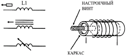
Rice. 2-24. Tunable inductors

Rice. 2-25. Coils with ferrite cores
When the coil operates in the radio frequency range, cores made of transformer iron or other metal are usually not used, since the eddy currents that occur in the core heat up the core, which leads to energy losses and significantly reduces the quality factor of the circuit. In this case, the cores are made of a special material - ferrite. Ferrite is a solid, ceramic-like mass, consisting of a very fine powder of iron or its alloy, where each metal particle is isolated from the others. Due to this, eddy currents do not occur in the core. The ferrite core is usually denoted by broken lines.
The next extremely common winding product is the transformer. In essence, a transformer is two or more inductors located in a common magnetic field. Therefore, the windings and the core of the transformer are depicted by analogy with the symbols of inductors (Fig. 2-26). An alternating magnetic field created by an alternating current flowing through one of the coils (primary winding) leads to the excitation of an alternating voltage in the remaining coils (secondary windings). The value of this voltage depends on the ratio of the number of turns in the primary and secondary windings. The transformer can be step-up, step-down or separating, but this property is usually not displayed on the graphic symbol in any way, signing the input or output voltage values \u200b\u200bnext to the winding terminals. In accordance with the basic principles of constructing circuits, the primary (input) winding of the transformer is shown on the left, and the secondary (output) windings are on the right.
Sometimes it is necessary to show which terminal is the beginning of the winding. In this case, a dot is placed near it. The windings are numbered in the diagram in Roman numerals, but the numbering of the windings is not always used. When the transformer has several windings, then to distinguish the conclusions, they are numbered with numbers on the transformer case, near the corresponding terminals, or they are made from conductors of different colors. On fig. Figure 2-26(C) is an example of an external view of a mains power supply transformer and a fragment of a circuit that uses a transformer with multiple windings.
On fig. 2-26(D) and 2-26(E) are buck and boost, respectively. autotransformers.
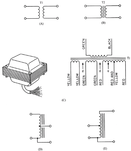
Rice. 2-26. Conditional graphic symbols of transformers
2.8. DIODES
The semiconductor diode is the simplest and one of the most commonly used semiconductor components, also called solid state components. Structurally, a diode is a semiconductor junction with two terminals - a cathode and an anode. A detailed discussion of the principle of operation of a semiconductor junction is beyond the scope of this book, so we will limit ourselves to describing the relationship between the diode device and its symbol.
Depending on the material used for the manufacture of the diode, the diode can be germanium, silicon, selenium, and by design point or planar, but on the diagrams it is indicated by the same symbol (Fig. 2-27).
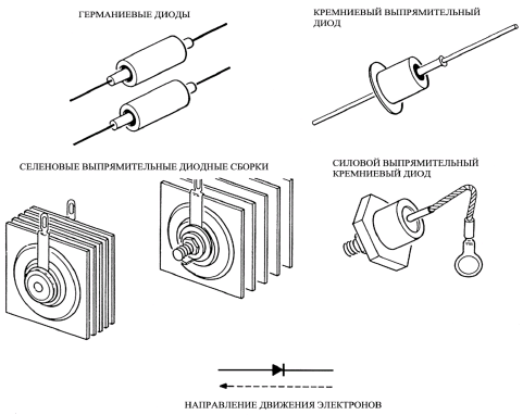
Rice. 2-27. Some options for the design of diodes
Sometimes the diode symbol is enclosed in a circle to show that the crystal is placed in a package (there are also unpackaged diodes), but this designation is rarely used now. In accordance with the domestic standard, diodes are depicted with an unfilled triangle and a through line passing through it, connecting the terminals.
The graphic designation of the diode has a long history. In the first diodes, a semiconductor junction was formed at the point of contact of a metal needle contact with a flat substrate made of a special material, such as lead sulfide.
In this design, the triangle depicts a needle contact.
Subsequently, planar diodes were developed in which a semiconductor junction occurs on the contact plane of n- and p-type semiconductors, but the designation of the diode remained the same.
We have already mastered enough conventions to easily read the simple circuit shown in Fig. 2-28 and understand how it works.
As expected, the diagram is built in the direction from left to right.
It begins with a picture of a mains plug in the "Western" standard, then comes a mains transformer and a diode rectifier built according to a bridge circuit, commonly called a diode bridge. The rectified voltage is supplied to some payload, conventionally indicated by the resistance Rn.
Quite often there is a variant of the image of the same diode bridge, shown in Fig. 2-28 right.
Which option is preferable to use is determined only by the convenience and visibility of the outline of a particular scheme.

Rice. 2-28. Two options for drawing a diode bridge circuit
The circuit under consideration is very simple, so understanding the principle of its operation does not cause difficulties (Fig. 2-29).
Consider, for example, the variant of the style shown on the left.
When a half-wave AC voltage from the transformer secondary is applied so that the top terminal is negative and the bottom is positive, electrons move in series through diode D2, the load, and diode D3.
When the polarity of the half wave is reversed, the electrons move through diode D4, the load, and diode DI. As you can see, regardless of the polarity of the operating half-wave of the alternating current, the electrons flow through the load in the same direction.
Such a rectifier is called full-wave, because both half-cycles of the AC voltage are used.
Of course, the current through the load will be pulsating, since the alternating voltage changes in a sinusoidal manner, passing through zero.
Therefore, in practice, most rectifiers use high-capacity smoothing electrolytic capacitors and electronic stabilizers.

Rice. 2-29. Movement of electrons through diodes in a bridge circuit
Most voltage stabilizers are based on another semiconductor device, which is very similar in design to a diode. In domestic practice, it is called zener diode, and in foreign circuitry a different name is adopted - zener diode(Zener Diode), by the name of the scientist who discovered the effect of tunneling breakdown p-n transition.
The most important property of a zener diode is that when a reverse voltage of a certain value is reached at its terminals, the zener diode opens and current begins to flow through it.
An attempt to further increase the voltage only leads to an increase in the current through the zener diode, but the voltage at its terminals remains constant. This voltage is called stabilization voltage. So that the current through the zener diode does not exceed the permissible value, they are connected in series with it quenching resistor.
There are also tunnel diodes, which, on the contrary, have the property of maintaining a constant current flowing through them.
Tunnel diodes are rare in common household appliances, mainly in nodes for stabilizing the current flowing through a semiconductor laser, for example, in CD-ROM drives.
But such nodes, as a rule, are not subject to repair and maintenance.
Much more common in everyday life are the so-called varicaps or varactors.
When a reverse voltage is applied to a semiconductor junction and it is closed, the junction has some capacitance, like a capacitor. A remarkable property of the p-n junction is that when the voltage applied to the junction changes, the capacitance also changes.
When making a transition using a certain technology, it is ensured that it has a sufficiently large initial capacity, which can vary over a wide range. That is why modern portable electronics do not use mechanical variable capacitors.
Optoelectronic semiconductor devices are extremely common. They can be quite complex in design, but in essence they are based on two properties of some semiconductor junctions. LEDs capable of emitting light when current flows through the junction, and photodiodes- change its resistance when changing the illumination of the transition.
LEDs are classified according to the wavelength (color) of the light emitted.
The color of the LED glow practically does not depend on the magnitude of the current flowing through the junction, but is determined by the chemical composition of the additives in the materials that form the junction. LEDs can emit both visible light and invisible infrared light. Recently, ultraviolet LEDs have been developed.
Photodiodes are also divided into those sensitive to visible light and those operating in the range invisible to the human eye.
A well-known example of a pair of LED-photodiode is a TV remote control system. The remote control has an infrared LED, and the TV has a photodiode of the same range.
Regardless of the range of radiation, LEDs and photodiodes are indicated by two generalized symbols (Fig. 2-30). These symbols are close to the current Russian standard, are very clear and do not cause difficulties.

Rice. 2-30. Designations of the main optoelectronic devices
If you combine an LED and a photodiode in one package, you get optocoupler. This is a semiconductor device, ideal for galvanic isolation of circuits. With it, you can transmit control signals without electrically connecting the circuits. Sometimes this is very important, for example, in switching power supplies, where it is necessary to galvanically separate the sensitive control circuit and high-voltage impulse circuits.
2.9. TRANSISTORS
Without a doubt, transistors are the most commonly used active components of electronic circuits. The transistor symbol does not reflect its internal structure too literally, but there is some relationship. We will not analyze in detail the principle of operation of the transistor, many textbooks are devoted to this. Transistors are bipolar And field. Consider the structure of a bipolar transistor (Fig. 2-31). A transistor, like a diode, consists of semiconductor materials with special additives. P- And p-type, but has three layers. The thin separating layer is called base, the other two - emitter And collector. The substitutive property of a transistor is that if the emitter and collector terminals are connected in series in an electrical circuit containing a power source and a load, then small changes in the current in the base-emitter circuit lead to significant, hundreds of times greater, changes in the current in the load circuit. Modern transistors are capable of driving voltages and load currents thousands of times greater than the voltages or currents in the base circuit.
Depending on the order in which the layers of semiconductor materials are arranged, there are bipolar transistors of the type rpr And npn. In a transistor graphic, this difference is reflected by the direction of the emitter terminal arrow (Figure 2-32). The circle indicates that the transistor has a housing. If it is necessary to indicate that a frameless transistor is used, as well as when depicting the internal circuit of transistor assemblies, hybrid assemblies or microcircuits, transistors are depicted without a circle.

Rice. 2-32. Graphic designation of bipolar transistors
When drawing circuits containing transistors, they also try to observe the principle "input on the left - output on the right."
On fig. 2-33, in accordance with this principle, three standard circuits for switching on bipolar transistors are simplified: (A) - with a common base, (B) - with a common emitter, (C) - with a common collector. In the image of the transistor, one of the variants of the character outline used in foreign practice is used.

Rice. 2-33. Options for turning on a transistor in a circuit
A significant disadvantage of the bipolar transistor is its low input impedance. A low-power signal source with a high internal resistance cannot always provide the base current necessary for the normal operation of a bipolar transistor. Field-effect transistors are deprived of this shortcoming. Their design is such that the current flowing through the load does not depend on the input current through the control electrode, but on the potential on it. Due to this, the input current is so small that it does not exceed the leakage in the insulating materials of the installation, so it can be neglected.
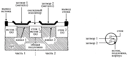
There are two main options for the design of a field effect transistor: with a control pn-junction (JFET) and a channel field-effect transistor with a metal-oxide-semiconductor structure (MOSFET, in Russian abbreviation MOS transistor). These transistors have different designations. First, let's get acquainted with the designation of the JFET transistor. Field-effect transistors are distinguished depending on the material from which the conductive channel is made. P- And p- type.
Pa fig. 2-34 shows the structure of the FET type and the legend of FETs with both types of conductivity.
This figure shows that gate, made of p-type material, located above a very thin channel of w-type semiconductor, and on both sides of the channel there are zones of "-type, to which the leads are connected source And runoff. The materials for the channel and gate, as well as the operating voltages of the transistor, are selected in such a way that, under normal conditions, the resulting rp- the junction is closed and the gate is isolated from the channel The load current flowing in series in the transistor through the source, channel, and drain pins depends on the gate potential.
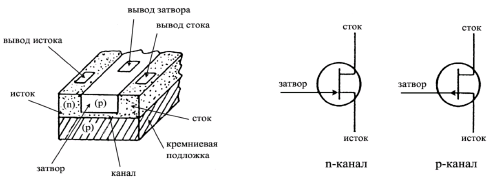
Rice. 2-34. Structure and designation of the channel field-effect transistor
A conventional field-effect transistor, in which the gate is isolated from the channel by a closed /w-junction, is simple in design and very common, but in the last 10-12 years its place has been gradually taken by field-effect transistors in which the gate is made of metal and isolated from the channel by a thin layer of oxide . Such transistors are commonly referred to abroad by the abbreviation MOSFET (Metal-Oxide-Silicon Field Effect Transistor), and in our country by the abbreviation MOS (Metal-Oxide-Semiconductor). The metal oxide layer is a very good dielectric.
Therefore, in MOS transistors there is practically no gate current, while in a conventional field-effect transistor, although it is very small, it is noticeable in some applications.
It is worth noting that MOSFETs are extremely sensitive to the effects of static electricity on the gate, since the oxide layer is very thin and exceeding the allowable voltage leads to breakdown of the insulator and damage to the transistor. When installing or repairing devices containing MOSFETs, special measures must be taken. One of the methods popular with radio amateurs is this: before mounting, the transistor leads are wrapped with several turns of a thin bare copper strand, which is removed with tweezers after soldering is completed.
The soldering iron must be grounded. Some transistors are protected by built-in Schottky diodes through which a charge of static electricity flows.
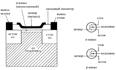
Rice. 2-35. Structure and designation of a rich MOSFET
Depending on the type of semiconductor from which the conductive channel is made, MOSFETs are distinguished. P- and p-type.
In the designation on the diagram, they differ in the direction of the arrow on the output of the substrate. In most cases, the substrate does not have its own output and is connected to the source and body of the transistor.
In addition, MOSFETs are enriched And depleted type. On fig. 2-35 shows the structure of an enriched n-type MOSFET. For a p-type transistor, the channel and substrate materials are reversed. A characteristic feature of such a transistor is that a conducting n-channel occurs only when the positive voltage at the gate reaches the required value. The variability of the conducting channel on the graphical symbol is reflected by a dashed line.
The structure of a depleted MOSFET and its graphic symbol are shown in fig. 2-36. The difference is that P- the channel is always present even when no voltage is applied to the gate, so the line between the source and drain pins is solid. The substrate is also most often connected to the source and ground and does not have its own output.
In practice, there are also double-gate Depleted-type MOSFETs, the design and designation of which are shown in fig. 2-37.
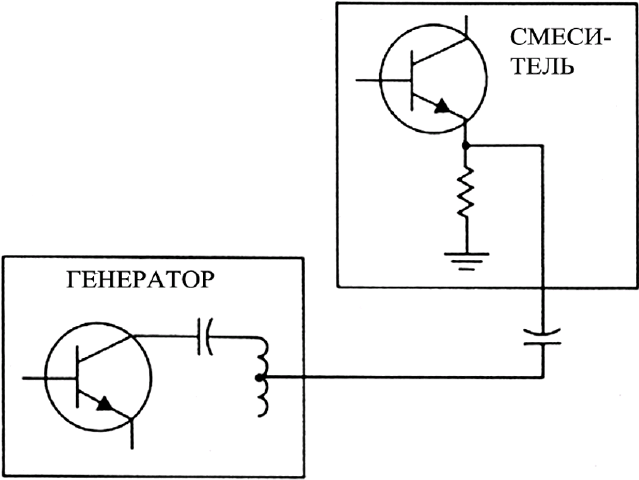
Such transistors are very useful when there is a need to combine signals from two different sources, for example, in mixers or demodulators.

Rice. 2-36. Structure and designation of a depleted MOSFET
Rice. 2-37. Structure and designation of a double-gate MOSFET
2.10. DINISTORS, THYRISTORS, TRIACTORS
Now that we have discussed the designations of the most popular semiconductor devices, diodes and transistors, let's get acquainted with the designations of some other semiconductor devices that are also often encountered in practice. One of them - diak or bidirectional diode thyristor(Figure 2-38).
In its structure, it is similar to two back-to-back diodes, except that the n-region is common and is formed rpr structure with two transitions. But, unlike a transistor, in this case both junctions have exactly the same characteristics, due to which this device is electrically symmetrical.
A rising voltage of either polarity is met with a relatively high resistance of the junction connected in reverse polarity until the reverse-biased junction avalanches. As a result, the resistance of the reverse transition drops sharply, the current flowing through the structure increases, and the voltage at the terminals decreases, forming a negative current-voltage characteristic.
Diacs are used to control any devices depending on the voltage, for example, to switch thyristors, turn on lamps, etc.

Rice. 2-38. Bidirectional diode thyristor (diac)
The following device is referred to abroad as a controlled silicon diode (SCR, Silicon Controlled Rectifier), and in domestic practice - triode thyristor, or trinistor(Figure 2-39). According to its internal structure, a triode thyristor is a structure of four alternating layers with different types of conductivity. This structure can be conditionally represented as two bipolar transistors of different conductivity.
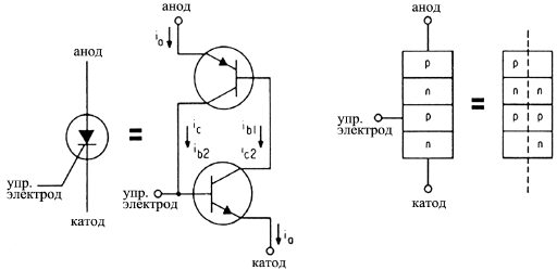
Rice. 2-39. Triode thyristor (SCR) and its designation
Trinistor works as follows. When properly turned on, the trinistor is connected in series with the load so that the positive potential of the power source is applied to the anode, and the negative potential to the cathode. In this case, no current flows through the trinistor.
When a positive voltage is applied to the control junction relative to the cathode and it reaches a threshold value, the SCR jumps into a conducting state with low internal resistance. Further, even if the control voltage is removed, the trinistor remains in a conducting state. The thyristor goes into the closed state only if the anode-cathode voltage becomes close to zero.
On fig. 2-39 shows a trinistor controlled by voltage with respect to the cathode.
If the trinistor is controlled by a voltage relative to the anode, the line representing the control electrode departs from the triangle representing the anode.
Due to their ability to remain open after the control voltage is turned off and the ability to switch high currents, trinistors are very widely used in power circuits, such as controlling electric motors, lighting lamps, powerful voltage converters, etc.
The disadvantage of triode thyristors is the dependence on the correct polarity of the applied voltage, which is why they cannot work in AC circuits.
Symmetrical triode thyristors or triacs, having a foreign name triac(Figure 2-40).
The graphic symbol of the triac is very similar to the symbol of the diac, but has a control electrode output. Triacs operate with either polarity of supply voltage applied to the main terminals and are used in a variety of applications where it is necessary to control an AC-powered load.

Rice. 2-40. Triac (triac) and its designation
Somewhat less commonly, bidirectional switches (balanced switches) are used, which, like the trinistor, have a structure of four alternating layers with different conductivity, but two control electrodes. The symmetrical key goes into a conducting state in two cases: when the anode-cathode voltage reaches the level of avalanche breakdown or when the anode-cathode voltage is less than the breakdown level, but voltage is applied to one of the control electrodes.

Rice. 2-41. Bidirectional switch (symmetrical key)
Oddly enough, but to designate a diac, a trinistor, a si-mistor and a bidirectional switch abroad, there are no generally accepted letter designations, and on the diagrams next to the graphic designation they often write a number that this component designates a specific manufacturer (which can be very inconvenient, since it generates confusion when there are several identical parts).
2.11. VACUUM ELECTRONIC LAMPS
At first glance, with the current level of development of electronics, it is simply inappropriate to talk about vacuum vacuum tubes (in everyday life - radio tubes).
But it's not. In some cases, vacuum tubes are still used today. For example, some hi-fi audio amplifiers are made using vacuum tubes because such amplifiers are said to have a special soft and clear sound that is not possible with transistor circuits. But this question is very complicated - just as the circuits of such amplifiers are complex. For a beginner radio amateur, this level, alas, is not available.
Much more often, radio amateurs are faced with the use of radio tubes in power amplifiers of radio transmitters. There are two ways to achieve high output power.
First, using high voltage at low currents, which is quite simple in terms of power supply - just use a step-up transformer and a simple rectifier containing diodes and smoothing capacitors.
And, secondly, operating with low voltages, but at high currents in the circuits of the output stage. This option requires a powerful stabilized power supply, which is quite complex, dissipates a lot of heat, bulky and very expensive.
Of course, there are specialized high-power high-frequency transistors operating at elevated voltages, but they are very expensive and rare.
In addition, they still significantly limit the allowable output power, and cascade circuits for switching on several transistors are difficult to manufacture and debug.
Therefore, transistor output stages in radio transmitters with a power of more than 15 ... 20 watts are usually used only in industrial equipment or in products of experienced radio amateurs.
On fig. 2-42 shows the elements from which the designations of various versions of vacuum tubes are "assembled". Let's take a quick look at the purpose of these elements:
(1) - Cathode heating filament.
If a directly heated cathode is used, it also denotes the cathode.
(2) - Indirectly heated cathode.
It is heated with a thread marked with the symbol (1).
(3) - Anode.
(4) - Mesh.
(5) - Reflective anode of indicator lamp.
Such an anode is coated with a special phosphor and glows under the influence of an electron flow. Currently, it is practically not used.
(6) - Forming electrodes.
Are intended for formation of a stream of electrons of the necessary form.
(7) - Cold cathode.
It is used in lamps of a special type and can emit electrons without heating, under the influence of an electric field.
(8) - A photocathode coated with a layer of a special substance that significantly increases the emission of electrons under the action of light.
(9) - Filler gas in gas-filled vacuum devices.
(10) - Housing. Obviously, there is no designation for a vacuum tube that does not contain a housing symbol. 
Rice. 2-42. Designations of various elements of radio tubes
The names of most radio tubes come from the number of basic elements. So, for example, a diode has only an anode and a cathode (the heating filament is not considered a separate element, since in the first radio tubes the heating filament was covered with a layer of a special substance and at the same time was the cathode; such radio tubes are still found today). The use of vacuum diodes in amateur practice is very rarely justified, mainly in the manufacture of high-voltage rectifiers for powering the already mentioned powerful output stages of transmitters. And even then, in most cases, they can be replaced by high-voltage semiconductor diodes.
On fig. 2-43 shows the main design options for radio tubes that can be encountered in the manufacture of amateur designs. In addition to the diode, this is a triode, tetrode and pentode. Double tubes are common, such as the double triode or double tetrode (Figure 2-44). There are also tubes that combine two different design options in one package, for example, a triode-pentode. It may happen that different parts of such a tube should be shown in different parts of the circuit diagram. Then the symbol of the body is not fully depicted, but partially. Sometimes one half of the hull symbol is shown as a solid line and the other half as a dotted line. All conclusions of the radio tubes are numbered clockwise, if you look at the lamp from the side of the conclusions. The corresponding pin numbers are put down on the diagram next to the graphic designation.

Rice. 2-43. Designations of the main types of radio tubes

Rice. 2-44. An example of the designation of composite radio tubes
And, finally, we will mention the most common electronic vacuum device that we all see in everyday life almost every day. This is a cathode ray tube (CRT), which, when it comes to a TV or computer monitor, is commonly called a kinescope. There are two ways to deflect the electron flow: using a magnetic field created by special deflecting coils, or using an electrostatic field created by deflecting plates. The first method is used in televisions and displays, as it allows the beam to be deflected to a large angle with good accuracy, and the second method is used in oscilloscopes and other measuring equipment, since it works much better at high frequencies and does not have a pronounced resonant frequency. An example of the designation of a cathode ray tube with an electrostatic deflection is shown in fig. 2-45. A CRT with electromagnetic deviation is depicted in much the same way, only instead of located inside deflector tubes side by side outside deflection coils. Very often, on the diagrams, the designations of the deflecting coils are not located next to the designation of the CRT, but where it is more convenient, for example, near the horizontal or vertical scan output stage. In this case, the purpose of the coil is indicated by the inscription Horizontal Deflection located nearby. Horizontal Yoke (line scan) or Vertical Deflection, Vertical Yoke (frame scan).

Rice. 2-45. Cathode ray tube designation
2.12. DISCHARGE LAMPS
Gas discharge lamps got their name in accordance with the principle of operation. It has long been known that between two electrodes placed in a rarefied gas medium, with a sufficient voltage between them, a glow discharge occurs, and the gas begins to glow. An example of gas-discharge lamps are lamps for advertising signs and indicator lamps for household appliances. Neon is most often used as a filling gas, so very often abroad gas-discharge lamps are denoted by the word "Neon", making the name of the gas a household name. In fact, gases can be different, up to mercury vapor, which gives ultraviolet radiation invisible to the eye ("quartz lamps").
Some of the most common designations for gas discharge lamps are shown in Fig. 2-46. Option (I) is very often used to indicate indicator lights that indicate that the mains power is on. Option (2) is more complicated, but similar to the previous one.
If the discharge lamp is sensitive to the polarity of the connection, the designation (3) is used. Sometimes the bulb of the lamp is coated from the inside with a phosphor, which glows under the influence of ultraviolet radiation that occurs during a glow discharge. By selecting the composition of the phosphor, it is possible to produce very durable indicator lamps with different luminous colors, which are still used in industrial equipment and are indicated by the symbol (4).
2-46. Common designations for gas discharge lamps
2.13. INCANDESCENT AND SIGNAL LIGHTS
The designation of the lamp (Fig. 2-47) depends not only on the design, but also on its purpose. Thus, for example, incandescent lamps in general, incandescent lighting lamps and incandescent lamps indicating plugging in, may be designated by the symbols (A) and (B). Signal lamps signaling any modes or situations in the operation of the device are most often denoted by the symbols (D) and (E). Moreover, it may not always be an incandescent lamp, so you should pay attention to the general context of the circuit. There is a special symbol (F) to indicate a flashing warning light. Such a symbol can be found, for example, in the electrical circuit of a car, where it is used to designate turn signal lamps.
Rice. 2-47. Designations of incandescent lamps and signal lamps
2.14. MICROPHONES, SOUND PRODUCERS
Sound-emitting devices can have a wide variety of designs based on various physical effects. In household appliances, the most common are dynamic loudspeakers and piezo emitters.
The generalized image of a loudspeaker in foreign circuitry coincides with the domestic UGO (Fig. 2-48, symbol 1). This symbol is used by default to designate dynamic loudspeakers, i.e. the most common loudspeakers in which the coil moves in a constant magnetic field and sets the diffuser in motion. Sometimes it becomes necessary to emphasize design features, and other designations are used. So, for example, the symbol (2) denotes a speaker in which the magnetic field is created by a permanent magnet, and the symbol (3) denotes a speaker with a special electromagnet. Such electromagnets were used in very powerful dynamic loudspeakers. Currently, DC biased loudspeakers are almost never used, because relatively inexpensive, powerful and large permanent magnets are commercially available.
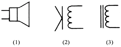
Rice. 2-48. Common Loudspeaker Designations
Widespread sound emitters also include bells and buzzers (beepers). The call, regardless of the destination, is depicted by the symbol (1) in Fig. 2-49. The buzzer is usually a high-pitched electromechanical system and is now very rarely used. On the contrary, the so-called beepers ("tweeters") are used very often. They are installed in cell phones, pocket electronic games, electronic watches, etc. In the vast majority of cases, the operation of beepers is based on the piezo-mechanical effect. A crystal of a special piezo-substance shrinks and expands under the influence of an alternating electric field. Sometimes beepers are used, which are similar in principle to dynamic loudspeakers, only very small. Recently, beepers are not uncommon, in which a miniature electronic circuit is built that generates sound. It is enough to apply a constant voltage to such a beeper so that it starts to sound. Regardless of the design features in most foreign circuits, beepers are denoted by the symbol (2), fig. 2-49. If the polarity of inclusion is important, it is indicated near the terminals.

Rice. 2-49. Designations of bells, buzzers and beepers
Headphones (in common parlance - headphones) have different designations in foreign circuitry that do not always coincide with the domestic standard (Fig. 2-50).
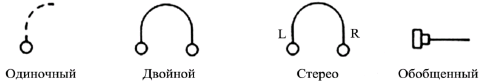
Rice. 2-50. Headphone designations
If we consider a circuit diagram of a tape recorder, music center or cassette player, then we will definitely meet the symbol of a magnetic head (Fig. 2-51). The UGOs shown in the figure are absolutely equivalent and represent a generalized designation.
If it is necessary to emphasize that we are talking about a reproducing head, then next to the symbol an arrow is shown pointing to the head.
If the head is recording, then the arrow is directed away from the head, if the head is universal, then the arrow is bidirectional, or is not displayed.

Rice. 2-51. Designations of magnetic heads
Common designations of microphones are shown in fig. 2-52. Such symbols denote either microphones in general, or dynamic microphones, structurally arranged like dynamic loudspeakers. If the microphone is electret, when the movable lining of the film capacitor perceives the sound vibrations of the air, then the symbol of a non-polar capacitor can be displayed inside the microphone symbol.
Very often there are electret microphones with a built-in preamplifier. Such microphones have three outputs, one of which is powered, and require respect for the polarity of the connection. If it is necessary to emphasize that the microphone has a built-in amplifying stage, a transistor symbol is sometimes placed inside the microphone designation.

Rice. 2-52. Graphic symbols for microphones
2.15. FUSES AND BREAKERS
The obvious purpose of fuses and circuit breakers is to protect the remaining components of the circuit from damage in the event of an overload or failure of one of the components. In this case, the fuses blow out and require replacement during repair. Protective circuit breakers, when the threshold value of the current flowing through them, goes into an open state, but most often they can be returned to their original state by pressing a special button.
When repairing a device that "does not show signs of life", first of all, check the mains fuses and the fuses at the output of the power source (rare, but found). If the device works normally after replacing the fuse, then the cause of the fuse blown was a power surge or other overload. Otherwise, a more serious repair is ahead.
Modern switching power supplies, especially in computers, very often contain self-healing semiconductor rectifiers. Such fuses usually take some time to restore conduction. This time is somewhat longer than the simple cooling time. The situation when a computer that did not even turn on suddenly starts working normally after 15-20 minutes is explained precisely by the restoration of the fuse.

Rice. 2-53. Fuses and circuit breakers

Rice. 2-54. Breaker with reset button
2.16. ANTENNAS
The location of the antenna symbol on the diagram depends on whether the antenna is receiving or transmitting. The receiving antenna is the input device, therefore it is located on the left, reading the receiver circuit begins with the antenna symbol. The transmitting antenna of the radio transmitter is placed on the right and completes the circuit. If a transmitter circuit is being built - a device that combines the functions of a receiver and a transmitter, then, according to the rules, the circuit is depicted in the receive mode and the antenna is most often placed on the left. If the device uses an external antenna connected via a connector, then very often only the connector is depicted, omitting the antenna symbol.
Very often generalized antenna symbols are used, fig. 2-55 (A) and (B). These symbols are used not only in circuit diagrams, but also in functional diagrams. Some graphic designations reflect the design features of the antenna. So, for example, in Fig. 2-55, the symbol (C) denotes a directional antenna, the symbol (D) denotes a dipole with a symmetrical feed, and the symbol (E) denotes a dipole with an unbalanced feed.
A wide variety of antenna designations used in foreign practice does not allow us to consider them in detail, but most of the designations are intuitive and do not cause difficulties even for beginner radio amateurs.

Rice. 2-55. Examples of designations for external antennas
3. STEP BY STEP BY YOURSELF
So, we briefly got acquainted with the main graphic designations of circuit elements. This is quite enough to start reading circuit diagrams, first the simplest, and then more complex. An unprepared reader may object: "Perhaps I can understand a circuit consisting of several resistors and capacitors and one or two transistors. But I will not be able to quickly understand a more complex circuit, such as a radio receiver." This is an erroneous statement.
Yes, indeed, many electronic circuits look very complex and intimidating. But, in fact, they consist of several functional blocks, each of which is a less complex circuit. The ability to divide a complex scheme into structural units is the first and main skill that the reader must acquire. Next, you should objectively assess the level of your own knowledge. Here are two examples. Let's say we are talking about repairing a VCR. Obviously, in this situation, a novice radio amateur is quite capable of finding a fault at the level of an open in the power circuits and even detecting missing contacts in the connectors of the ribbon cables of the board-to-board connections. This will require at least a rough idea of the functional diagram of the VCR and the ability to read the circuit diagram. Repair of more complex nodes will be within the power of only an experienced master, and it is better to immediately abandon attempts to randomly fix a malfunction, since there is a high probability of aggravating the malfunction with unskilled actions.
Another thing is when you are going to repeat a relatively simple amateur radio design. As a rule, such electronic circuits are accompanied by detailed descriptions and wiring diagrams. If you know the system of symbols, then you can easily repeat the design. Surely later you will want to make changes to it, improve it or adjust it to the available components. And the ability to dismember the circuit into constituent functional blocks will play a huge role. For example, you can take a circuit that was originally designed for battery operation and connect to it a mains source "borrowed" from another circuit. Or use another low-frequency amplifier in the radio - there can be many options.
3.1. CONSTRUCTION AND ANALYSIS OF A SIMPLE SCHEME
To understand the principle by which the finished circuit is mentally divided into functional nodes, we will do the reverse work: from the functional nodes we will build a circuit of a simple detector receiver. The RF part of the circuit, which separates the baseband signal from the input RF signal, consists of an antenna, a coil, a variable capacitor, and a diode (Figure 3-1). This circuit fragment can be called simple, right? In addition to the antenna, it consists of only three parts. Coil L1 and capacitor C1 form an oscillatory circuit, which, from the many electromagnetic oscillations received by the antenna, selects oscillations of only the desired frequency. Detection of oscillations (isolation of the low-frequency component) occurs using the diode D1.

Rice. 3-1. RF part of the receiver circuit
To start listening to radio broadcasts, it is enough to add high-impedance headphones connected to the output terminals to the circuit. But we are not satisfied with this. We want to listen to radio broadcasts through the loudspeaker. The signal directly at the output of the detector has a very low power, so in most cases one amplifying stage is not enough. We decide to use a pre-amplifier, the circuit of which is shown in Fig. 3-2. This is another functional block of our radio. Please note that a power source has appeared in the circuit - battery B1. If we want to power the receiver from a network source, then we must depict either the terminals for connecting it, or the diagram of the source itself. For simplicity, we restrict ourselves to the battery.
The preamplifier circuit is very simple, it can be drawn in a couple of minutes, and mounted in about ten.
After combining the two functional nodes, the diagram of Fig. 3-3. At first glance, it has become more difficult. Is it so? It is composed of two fragments that did not seem difficult at all separately. The dotted line shows where the imaginary dividing line between functional nodes passes. If you understand the schemes of the two previous nodes, then it will not be difficult to understand the general scheme. Please note that in the diagram in Fig. 3-3, the numbering of some elements of the preamplifier has changed. Now they are part of the general scheme and are numbered in the general order for this particular scheme.

Rice. 3-2. Receiver preamplifier
The signal at the output of the preamplifier is stronger than at the output of the detector, but not enough to connect a loudspeaker. It is necessary to add another amplifying stage to the circuit, due to which the sound in the speaker will be quite loud. One of the possible variants of the functional unit is shown in Fig. 3-4.
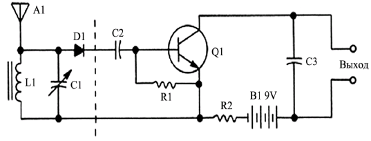
Rice. 3-3. Intermediate version of the receiver circuit

Rice. 3-4. Receiver output amplifier stage
Let's add an output amplifier stage to the rest of the circuit (Figure 3-5).
We connect the output of the preamplifier to the input of the final stage. (We can't feed the signal directly from the detector to the output stage because the signal is too weak without preamplification.)
You may have noticed that the power battery was shown in both the preamplifier and power amplifier diagrams, but only once in the final diagram.
In this circuit, there is no need for separate power supplies, so both amplifier stages in the final circuit are connected to the same source.
Of course, in the form in which the circuit is shown in Fig. 3-5, it is unsuitable for practical use. The values of resistors and capacitors, the alphanumeric designations of the diode and transistors, the winding data of the coil are not indicated, there is no volume control.
However, this scheme is very close to those used in practice.
With the assembly of the radio receiver in a similar way, many radio amateurs begin their practice.

Rice. 3-5. The final circuit of the radio
We can say that the main process in the development of circuits is combination.
First, at the level of the general idea, blocks of the functional diagram are combined.
Then individual electronic components are combined, from which simple functional units of the circuit are obtained.
They, in turn, are combined into a more complex overall scheme.
Schemes can be combined with each other to build a functionally complete product.
Finally, the products can be combined to build a hardware system such as a home theater system.
3.2. COMPLEX CIRCUIT ANALYSIS
With some experience, analysis and combination are quite accessible even to a novice radio amateur or a home master when it comes to assembling or repairing simple household circuits.
You just need to remember that skill and understanding comes only with practice. Let's try to analyze a more complex circuit shown in Fig. 3-6. As an example, we use the circuit of an amateur radio AM transmitter for the 27 MHz band.
This is a very real scheme, such or a similar scheme can often be found on amateur radio sites.
It is deliberately left in the form in which it is given in foreign sources, with the original designations and terms preserved. To facilitate understanding of the circuit by novice radio amateurs, it is already divided by solid lines into functional blocks.
As expected, we will start the consideration of the scheme from the upper left corner.
The first section located there contains a microphone preamplifier. Its simple circuit contains a single p-channel FET whose input impedance matches well with the output impedance of an electret microphone.
The microphone itself is not shown in the diagram, only the connector for connecting it is shown, and the microphone type is indicated next to the text. Thus, a microphone can be from any manufacturer, with any alphanumeric designation, as long as it is electret and does not have a built-in amplifying stage. In addition to the transistor, the preamplifier circuit contains several resistors and capacitors.
The purpose of this circuit is to amplify the weak microphone output signal to a level sufficient for further processing.
The next section is the ULF, which consists of an integrated circuit and several external parts. ULF amplifies the audio frequency signal coming from the output of the pre-amplifier, as was the case with a simple radio receiver.
The amplified audio signal enters the third section, which is a matching circuit and contains a modulating transformer T1. This transformer is a matching element between the low-frequency and high-frequency parts of the transmitter circuit.
The low frequency current flowing in the primary winding causes changes in the collector current of the high frequency transistor flowing through the secondary winding.
Next, let's move on to the consideration of the high-frequency part of the circuit, starting from the lower left corner of the drawing. The first high-frequency section is a quartz reference oscillator, which, thanks to the presence of a quartz resonator, generates radio frequency oscillations with good frequency stability.
This simple circuit contains only one transistor, several resistors and capacitors, and a high-frequency transformer, consisting of coils L1 and L2, placed on a single frame with an adjustable core (it is shown by an arrow). From the output of the L2 coil, a high-frequency signal is fed to a high-frequency power amplifier. The signal produced by the crystal oscillator is too weak to feed into the antenna.
And, finally, from the output of the RF amplifier, the signal enters the matching circuit, whose task is to filter out harmonic spurious frequencies that occur when the RF signal is amplified, and match the output impedance of the amplifier with the input impedance of the antenna. The antenna, like the microphone, is not shown in the diagram.
It can be of any design intended for this range and output power level.
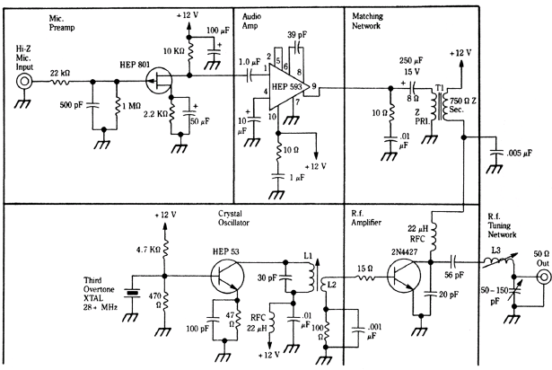
Rice. 3-6. Amateur AM transmitter circuit
Take a look at this diagram again. Perhaps it no longer seems difficult to you? Of the six segments, only four contain active components (transistors and a chip). This supposedly difficult to understand circuit is actually a combination of six different simple circuits, all of which are easy to understand.
The correct order of drawing and reading diagrams has a very deep meaning. It turns out that it is very convenient to assemble and configure the device in the order in which it is convenient to read the diagram. For example, if you have little to no experience in assembling electronic devices, the transmitter just discussed is best assembled starting with a microphone amplifier, and then - in stages, checking the operation of the circuit at each stage. This will save you from the tedious search for an installation error or a faulty part.
As for our transmitter, all fragments of its circuit, subject to serviceable parts and proper installation, should start working immediately. Settings require only the high-frequency part, and then after the final assembly.
First of all, we assemble a microphone amplifier. We check the correct installation. We connect an electret microphone to the connector and apply power. With the help of an oscilloscope, we make sure that undistorted amplified sound vibrations are present at the source terminal of the transistor when something is said into the microphone.
If this is not the case, it is necessary to replace the transistor, protecting it from breakdown by static electricity.
By the way, if you have a microphone with a built-in amplifier, then this stage is not needed. You can use a connector with three pins (to supply power to the microphone) and apply the signal from the microphone through the isolation capacitor directly to the second stage.
If 12 volts is too high to power the microphone, add a simple microphone power supply from a series-connected resistor and a zener diode rated for the desired voltage (usually 5 to 9 volts).
As you can see, even at the first steps there is room for creativity.
Next, we assemble the second and third sections of the transmitter in order. After we have made sure that there are amplified sound vibrations on the secondary winding of the transformer T1, we can consider the assembly of the low-frequency part to be completed.
The assembly of the high-frequency part of the circuit begins with a master oscillator. If there is no RF voltmeter, frequency meter or oscilloscope, the presence of generation can be verified using a receiver tuned to the desired frequency. You can also connect a simple indicator of the presence of high-frequency oscillations to the output of the coil L2.
Then the output stage is assembled, the matching circuit is connected, the equivalent of the antenna is connected to the antenna connector and the final adjustment is made.
The procedure for setting up the RF cascades. especially weekends, is usually described in detail by the authors of the schemes. For different schemes, it can be different and is beyond the scope of this book.
We have looked at the relationship between the structure of a circuit and the order in which it is assembled. Of course, the schemes are not always so clearly structured. However, you should always try to break down a complex circuit into functional nodes, even if they are not explicitly distinguished.
3.4. REPAIR OF ELECTRONIC DEVICES
As you can see, we have considered assembly transmitter in the order "from input to output". So it is more convenient to debug the circuit.
But troubleshooting when repairing, it is customary to conduct in the reverse order, "from the exit to the entrance." This is due to the fact that the output stages of most circuits operate with relatively large currents or voltages and fail much more often. For example, in the same transmitter, the reference crystal oscillator is practically not subject to malfunctions, while the output transistor can easily fail due to overheating in the event of an open or short circuit in the antenna circuit. Therefore, if the transmitter radiation is lost, first of all, the output stage is checked. They do the same with IF amplifiers in tape recorders, etc.
But before checking the components of the circuit, you need to make sure that the power supply is working and that the supply voltages are supplied to the main board. Simple, so-called linear, power supplies can also be tested "from input to output", starting with the mains plug and fuse. Any experienced radio technician will tell you how much household equipment is brought into the workshop because of a faulty power cord or blown fuse. The situation with pulsed sources is much more complicated. Even the simplest switching power supply circuits can contain very specific radio components and are usually covered by feedback loops and mutually affecting adjustments. A single fault in such a source often leads to the failure of many components. Inept actions can aggravate the situation. Therefore, the repair of the pulse source must be carried out by a qualified specialist. In no case should you neglect the safety requirements when working with electrical appliances. They are simple, well-known and repeatedly described in the literature.
|
GOST 19880-74 |
Electrical engineering. Basic concepts. |
|
GOST 1494-77 |
Letter designations. |
|
GOST 2.004-79 |
Rules for the execution of design documents on printing and graphic output devices of a computer. |
|
GOST 2.102-68 |
Types and completeness of design documents. |
|
GOST 2.103-68 |
Development stages. |
|
GOST 2.104-68 |
Basic inscriptions. |
|
GOST 2.105-79 |
General requirements for text documents. |
|
GOST 2.106-68 |
Text documents. |
|
GOST 2.109-73 |
Basic requirements for drawings. |
|
GOST 2.201-80 |
Designations of products and design documents. |
|
GOST 2.301-68 |
Formats. |
|
GOST 2.302-68 |
Scales. |
|
GOST 2.303-68 |
Lines. |
|
GOST 2.304-81 |
Drawing fonts. |
|
GOST 2.701-84 |
Schemes. Types and types. General performance requirements. |
|
GOST 2.702-75 |
Rules for the implementation of electrical circuits. |
|
GOST 2.705-70 |
Rules for the implementation of electrical circuits, windings and products with windings. |
|
GOST 2.708-81 |
Rules for the implementation of electrical circuits of digital computer technology. |
|
GOST 2.709-72 |
Circuit designation system in electrical circuits. |
|
GOST 2.710-81 |
Alphanumeric designations in electrical circuits. |
|
GOST 2.721-74 |
Designations for general use. |
|
GOST 2.723-68 |
Inductors, chokes, transformers, autotransformers and magnetic amplifiers. |
|
GOST 2.727-68 |
Dischargers, fuses. |
|
GOST 2.728-74 |
Resistors, capacitors. |
|
GOST 2.729-68 |
Electrical measuring instruments. |
|
GOST 2.730-73 |
Semiconductor devices. |
|
GOST 2.731-81 |
Electrovacuum devices. |
|
GOST 2.732-68 |
Sources of light. |
Radio elements (radio components) are electronic components assembled into components of digital and analog equipment. Radio components have found their application in video equipment, sound devices, smartphones and phones, TVs and measuring instruments, computers and laptops, office equipment and other equipment.
Types of radio elements
The radio elements connected by means of conductor elements together form an electrical circuit, which can also be called a "functional assembly". A set of electrical circuits from radio elements, which are located in a separate common housing, is called a microcircuit - an electronic assembly, it can perform many different functions.
All electronic components used in household and digital appliances are classified as radio components. It is rather problematic to list all the subspecies and types of radio components, since you get a huge list that is constantly expanding.
To designate radio components in the diagrams, both graphic symbols (UGO) and alphanumeric characters are used.
According to the method of action in the electrical circuit, they can be divided into two types:
- Active;
- Passive.
active type
Active electronic components are completely dependent on external factors, under the influence of which they change their parameters. It is this group that brings energy to the electrical circuit.

The following main representatives of this class are distinguished:
- Transistors are a semiconductor triode that, through an input signal, can control and control the electrical voltage in a circuit. Before the advent of transistors, their function was performed by vacuum tubes, which consumed more electricity and were not compact;
- Diode elements are semiconductors that conduct electricity in only one direction. They have one electrical junction and two leads, they are made of silicon. In turn, diodes are divided by frequency range, design, purpose, transition dimensions;
- Microcircuits are composite components in which capacitors, resistors, diode elements, transistors and other things are integrated into a semiconductor substrate. They are designed to convert electrical impulses and signals into digital, analog and analog-to-digital information. They can be produced without or with a housing.

There are many more representatives of this class, but they are used less frequently.
passive type
Passive electronic components do not depend on the flowing electric current, voltage and other external factors. They can either consume or store energy in an electrical circuit.
The following radio elements can be distinguished in this group:
- Resistors are devices that redistribute electric current between the constituent elements of a microcircuit. They are classified according to manufacturing technology, installation and protection method, purpose, current-voltage characteristic, the nature of the change in resistance;
- Transformers are electromagnetic devices that are used to convert, while maintaining the frequency, one alternating type electric current system to another. Such a radio component consists of several (or one) wire coils covered by a magnetic flux. Transformers can be matching, power, pulse, separating, as well as current and voltage devices;
- Capacitors - an element that serves to accumulate electric current and then release it. They consist of several electrodes separated by dielectric elements. Capacitors are classified according to the type of dielectric components: liquid, solid organic and inorganic, gaseous;
- Inductive coils are conductor devices that serve to limit alternating type electric current, suppress interference and accumulate electricity. The conductor is placed under the insulating layer.

Marking of radio components
The marking of radio components is usually made by the manufacturer and is located on the product case. Labeling of such elements can be:
- symbolic;
- color;
- symbolic and color at the same time.
Important! The labeling of imported radio components may differ significantly from the labeling of domestically produced elements of the same type.
On a note. Each radio amateur, when trying to decipher one or another radio component, resorts to a reference book, since it is not always possible to do this from memory due to the huge model variety.

The designation of radio elements (marking) of European manufacturers often occurs according to a specific alphanumeric system consisting of five characters (three numbers and two letters for products for general use, two numbers and three letters for special equipment). The numbers in such a system determine the technical parameters of the part.
European marking system for semiconductors of wide distribution
| 1st letter - material coding | |
|---|---|
| A | The main component is germanium |
| B | Silicon |
| C | Compound of gallium and arsenic - gallium arsenide |
| R | Cadmium sulfide |
| 2nd letter - type of product or its description | |
| A | Low power diode element |
| B | Varicap |
| C | Low power transistor operating at low frequencies |
| D | Powerful transistor operating at low frequencies |
| E | tunnel diode component |
| F | Low power high frequency transistor |
| G | More than one device in one housing |
| H | Magnetic diode |
| L | Powerful transistor operating at high frequency |
| M | Hall Sensor |
| P | Phototransistor |
| Q | Light diode |
| R | Low Power Switching Appliance |
| S | Switching transistor low power |
| T | Powerful switching device |
| U | Power switching transistor |
| X | Multiplier diode element |
| Y | High Power Rectifier Diode |
| Z | zener diode |
Designation of radio components on wiring diagrams
Due to the fact that there are a huge variety of different electronic components, the norms and rules for their graphic designation on a microcircuit were adopted at the legislative level. These regulations are called GOSTs, which contain comprehensive information on the type and size parameters of the graphic image and additional symbolic clarifications.
Important! If a radio amateur draws up a diagram for himself, then GOSTs can be neglected. However, if the electrical circuit being drawn up will be submitted for examination or verification to various commissions and government agencies, then it is recommended to check everything with fresh GOSTs - they are constantly supplemented and changed.

The designation of radio components of the "resistor" type, located on the board, looks like a rectangle in the drawing, next to it with the letter "R" and a number - a serial number. For example, "R20" means that the resistor in the circuit is the 20th in a row. Inside the rectangle, its working power can be written, which it can dissipate for a long time without collapsing. The current passing through this element dissipates a specific power, thereby heating it. If the power is greater than the nominal, then the radio product will fail.

Each element, like a resistor, has its own requirements for the outline on the circuit drawing, symbolic and numerical symbols. To search for such rules, you can use a variety of literature, reference books and numerous Internet resources.
Any radio amateur must understand the types of radio components, their marking and conditionally graphic designation, since it is such knowledge that will help him correctly compose or read the existing circuit.
Video
Cylindrical battery polarity
and conditional graphic designation. batteries on the diagram in accordance with GOST.
The designation of the battery on electrical diagrams contains a short line indicating the negative pole and a long line indicating the positive pole. A single battery used to power the device is denoted in the diagrams with the Latin letter G, and a battery consisting of several batteries with the letters GB.
Examples of using the designation of batteries in diagrams.
The simplest conventional graphic designation of a battery or accumulator in accordance with GOST is used in Scheme 1. A more informative battery designation in accordance with GOST is used in Scheme 2, here the number of batteries in a group battery is shown, the battery voltage and positive pole are indicated. GOST allows using the battery designation used in Scheme 3.
BATTERY CONNECTION DIAGRAM
Often in household appliances there is the use of several cylindrical batteries. The inclusion of a different number of series-connected batteries allows you to get power supplies that provide different voltages. Such a battery power supply gives a voltage equal to the sum of the voltages of all incoming batteries.
Serial connection of three batteries with a voltage of 1.5 volts provides a supply voltage of the device of 4.5 volts.
When the batteries are connected in series, the current supplied to the load is reduced due to the increasing internal resistance of the power supply.
Connecting batteries to the TV remote control.
For example, we are faced with the sequential inclusion of batteries when replacing them in the TV remote control.
Parallel connection of batteries is rarely used. The advantage of parallel connection is to increase the load current collected in this way by the power source. The voltage of the batteries connected in parallel remains the same, equal to the nominal voltage of one battery, and the discharge current increases in proportion to the number of combined batteries. Several weak batteries can be replaced with one more powerful one, so it is pointless to use parallel connection for low-power batteries. In parallel, it makes sense to turn on only powerful batteries, due to the absence or high cost of batteries with an even higher discharge current.
Parallel connection of batteries.
This inclusion has a drawback. Batteries cannot have exactly the same voltage across the contacts when the load is off. For one battery, this voltage can be 1.45 volts, and for the other 1.5 volts. This will cause current to flow from the battery with the higher voltage to the battery with the lower one. Discharge will occur when batteries are installed in the device compartments with the load disconnected. In the future, with such a switching scheme, self-discharge occurs faster than with sequential switching.
By combining series and parallel connection of batteries, you can get different power of the battery power supply.


Designation of radio components on the diagram
This article provides appearance and schematic designation radio components
Every novice radio amateur probably saw externally radio components and possibly circuits, but what is on the circuit you have to think or look for a long time, and only somewhere he can read and see new words for himself such as resistor, transistor, diode, etc. But what about they are designated. We will analyze in this article. And so we went.
1.Resistor
Most often, you can see a resistor on the boards and circuits, since there are most of them on the boards.
Resistors are both constant and variable (you can adjust the resistance with a knob)
One of the permanent pictures resistor below and designation permanent And variable on the diagram.


Where does the variable resistor look like? This is another picture below. I apologize for writing this article.

2.Transistor and its designation
A lot of information has been written about their functions, but since the topic is about notation. Let's talk about notation.
Transistors are bipolar, and polar, PNP and NPN transitions. All this is taken into account when soldering to the board, and in the circuits. See the picture, you will understand
Transistor designation npn transition npn
![]()
uh this emitter, k it collector, and B is base.Transistors pnp transitions will differ in that the arrow will not be from the base but to the base. For more details, one more picture
![]()
There are also bipolar and field-effect transistors, the designation on the field-effect transistor circuit is similar, but different. Since there is no emitter and collector base, but there is C - drain, I - source, Z - gate

And finally, about transistors, how do they actually look?

In general, if a part has three legs, then 80 percent of what it is is a transistor.
If you have a transistor and do not know what kind of transition it is and where the collector, base, and all other information is, then look in the transistor reference book.
Capacitor, appearance and designation
Capacitors are polar and non-polar, a plus is attached to the polar ones in the circuit, since it is for direct current, and non-polar, respectively, for alternating current.
They have a certain capacitance in uF (microfarads) and are designed for a certain voltage in volts. All this can be read on the capacitor case

Microcircuits, appearance designation on the diagram
Uff dear readers, there are just a huge number of these in the world, starting from amplifiers and ending with TVs