Where non-flammable fabrics are used www.algo-textile.ru. Mosquito nets accessories for mosquito nets 2-sklad.ru.
PCI and PCI-X
PCI and PCI-X buses
Introduction
PCI and PCI-X buses are the main I / O expansion buses in modern computers; for connecting video adapters, they are complemented by an AGP port. Expansion Bus is a system-level connection that allows adapters and peripheral controllers to directly use the computer's system resources - memory and I / O address space, interrupts, and direct memory access. Devices connected to expansion buses can manage these buses themselves, gaining access to the rest of the computer's resources. Expansion buses are mechanically implemented as slots (slotted connectors) or pin connectors; they are characterized by a small length of conductors, that is, they are purely local, which makes it possible to achieve high operating speeds. These buses may not be output to connectors, but are used to connect devices in integrated motherboards.
Initially, the PCI bus was introduced as an add-on (mezzanine bus) to systems with an ISA bus. It was designed for Pentium processors, but worked well with i486 processors. Later PCI became the central bus for some time: it was connected to the processor bus by a high-performance bridge ("north" bridge) that was part of the motherboard chipset. The rest of the I / O expansion buses (ISA / EISA or MCA), as well as the local ISA-like X-BUS and LPC interface, to which the motherboard chips are connected (ROM BIOS, interrupt controllers, keyboards, DMA, COM and LPT ports, floppy disk drives, etc. other "little things"), connected to the PCI bus through the "south" bridge. In modern motherboards with a "hub" architecture, the PCI bus has been moved to the periphery, without infringing on the power of the communication channel with the processor and memory, but also without loading transit traffic from devices on other buses.
The PCI bus is synchronous - all signals are latched on the positive edge (edge) of the CLK signal. The nominal clock frequency is considered to be 33.3 MHz; if necessary, it can be lowered. Starting from PCI 2.1, it is allowed to increase the frequency to 66.6 MHz if all devices on the bus agree. In PCI-X, the frequency can reach 133 MHz.
PCI uses a 32-bit parallel multiplexed address / data (AD) bus. The specification defines the possibility of expanding the bit depth up to 64 bits; PCI-X version 2.0 also defines a 16-bit bus option. With a bus frequency of 33 MHz, the theoretical bandwidth reaches 132 MB / s for a 32-bit bus and 264 MB / s for a 64-bit one; at a synchronization frequency of 66 MHz - 264 MB / s and 528 MB / s, respectively. However, these peaks are only reached during packet transmission: due to protocol overhead, the actual average bus bandwidth is lower.
Comparative characteristics of PCI and PCI-X buses and other expansion buses for PC-compatible computers are shown in Table. 1.1. The ISA bus is leaving desktop computers, but it retains its position in industrial and embedded computers, both in the traditional slot and in the "sandwich" PC / 104 version. Notebook computers widely use PCMCIA slots with PC Card and Card Bus. The LPC bus is a modern, low-cost means of connecting low-resource devices to the motherboard.
| Tire | Peak throughput MB / s | DMA channels | Bus-Master | ACFG | Bit depth of data | Address width | Frequency MHz |
| ISA-8 | 4 | 3 | - | - | 8 | 20 | 8 |
| ISA-16 | 8 |
7 |
+ |
- |
16 |
24 |
8 |
| Lpc | 6,7 |
7 |
+ |
- |
8/16/32 |
32 |
33 |
| EISA |
33,3 | 7 | + |
+ |
32 |
32 |
8,33 |
| MCA-16 |
16 |
- |
+ |
+ |
16 |
24 |
10 |
| MCA-32 |
20 |
- |
+ |
+ |
32 |
32 |
10 |
| VLB |
132 |
- |
(+) |
- |
32/64 |
32 |
33-50(66) |
| PCI |
133-533 |
- |
+ |
+ |
32/64 |
32/64 |
33/66 |
| PCI-X |
533-4256 |
- |
+ |
+ |
16/32/64 |
32/64 |
66-133 |
| PCI Express |
496-15872 |
- |
+ |
+ |
1/2/4/8/12/16/32 |
32/64 |
2.5 GHz |
| AGP 1x / 2x / 4x / 8x |
266/533/1066/2132 |
- |
+ |
+ |
32 |
32/64 |
66 |
| PCMCIA |
10/22 |
+ |
- |
+ |
8/16 |
26 |
10 |
| Card Bus | 132 | - | + | + | 32 | 32 | 33 |
ACFG1-Support for automatic configuration. For ISA, PnP is a late add-on implemented by adapters and software.
PCI and PCI-X bus signaling protocol
The exchange of information via the PCI and PCI-X bus is organized in the form of transactions - logically completed exchange operations. A typical transaction involves two devices — the initiator of the exchange (initiator), which is also the master device (master), and the target device (CO, target)), which is also the slave. The rules for the interaction of these devices are determined by the PCI bus protocol. The device can monitor transactions on the bus without being a participant (without entering any signals); the snooping term corresponds to the snooping mode. There is a special type of transaction (Special Cycle) - broadcast, in which the initiator protocol does not interact with any of the devices. Each transaction executes one command, usually reading or writing data to the specified address. The transaction begins with the address phase, in which the initiator specifies the command and the target address. Further, data phases can follow, in which one device (data source) puts data on the bus, and another (sink) reads it. Transactions that have multiple data phases are called batch transactions. There are also single transactions (with one data phase). A transaction can complete without data phases if the target device (or initiator) is not ready to exchange. An attribute phase has been added to the PCI-X bus, in which additional information about a transaction is transmitted.
PCI and PCI-X bus signaling protocol
The composition and purpose of the bus interface signals is disclosed in the table below. The states of all signal lines are perceived by the positive slope of CLK, and it is these moments in the further description that are meant as bus cycles (in the figures they are marked with vertical dashed lines). Different bus devices control the same signal lines at different times, and correct (conflict-free) "handover" requires that there is a period of time during which no device controls the line. In time charts, this event - the so-called “turnaround” - is indicated by a pair of semicircular arrows.
Table. PCI bus signals
| Signal |
Appointment |
| AD | Address / Data - multiplexed address / data bus. At the beginning of the transaction, the address is transmitted, in subsequent clock cycles - the data |
| C / B # | Command / Byte Enable - command / enable access to bytes. The command defining the type of the next bus cycle is set by a four-bit code in the address phase |
| FRAME # |
Frame. The introduction of a signal marks the beginning of the transaction (address phase), removal of the signal indicates that the subsequent data transfer cycle is the last in the transaction |
| DEVSEL # |
Device Select - the device is selected (the response of the control center to the transaction addressed to it) |
| IRDY # |
Initiator Ready - readiness of the master to exchange data |
| TRDY # |
Target Ready - readiness of the control center for data exchange |
| STOP # |
MC request to the master to stop the current transaction |
| LOCK # |
Bus lock (lock) signal to ensure complete operation. Used by a bridge that requires multiple PCI transactions to complete a single operation |
| REQ # |
Request - a request from the master to seize the bus |
| GNT # |
Grant - Granting the bus control to the master |
| PAR |
Parity - common parity bit for AD and C / BE lines # |
| PERR # |
Parity Error - a signal about a parity error (for all cycles, except for special ones). Generated by any device that detects an error |
| PME # |
Power Management Event - a signal about events causing a change in the consumption mode (additional signal introduced in PCI 2.2) |
| CLKRUN # |
Clock running - the bus is running at the nominal clock frequency. Removing the signal means slowing down or stopping synchronization in order to reduce consumption (for mobile applications) |
| PRSN # |
Present - indicators of the board presence, encoding the request for power consumption. On the expansion card, one or two indicator lines are connected to the GND bus, which is perceived by the motherboard |
| RST # |
Reset - reset all registers to their initial state (using the "Reset" button and on reboot) |
| IDSEL |
Initialization Device Select - device selection in configuration read and write cycles; these cycles are answered by a device that detects a high signal level on this line |
| SERR # |
System Error - system error. An address or data parity error in a special loop, or other catastrophic error detected by the device. Activated by any PCI device and calls the NMI |
| REQ64 # |
Request 64 bit - a request for a 64-bit exchange. The signal is introduced by a 64-bit initiator, in time it coincides with the FRAME # signal. During the end of the reset (with the RST # signal) it signals to the 64-bit device that it is connected to the 64-bit bus. If the 64-bit device does not detect this signal, it must reconfigure to 32-bit mode by disabling the high-byte buffers |
| ACK64 # |
Confirmation of 64-bit exchange. The signal is entered by a 64-bit MC, which recognized its address, simultaneously with DEVSEL #. The absence of this confirmation will force the initiator to perform the exchange with 32-bit |
| INTA #, INTB #, INTC #, INTD # |
Interrupt A, B, C, D - interrupt request lines, level sensitivity, active level - low, which allows separability (sharing) of lines |
| CLK |
Clock - the clock frequency of the bus. Should be in the range of 20-33 MHz, starting from PCI 2.1 it can be up to 66 MHz, in PCI-X up to 100 and 133 MHz |
| M66EN |
66MHz Enable - resolution of the clock frequency up to 66 MHz (on 33 MHz cards it is grounded, at 66 MHz it is free) |
| PCIXCAP (38B) |
Possibilities of PCI-X: on PCI cards - grounded, on PCI-X133 it is connected to ground through a 0.01 μF capacitor, on PCI-X66 - by a parallel RC chain of 10 kOhm, 0.01 μF. |
| SDONE |
Snoop Done - signal the completion of the snoop cycle for the current transaction. A low level indicates an incomplete memory-cache tracking cycle. Optional signal, used only by cached bus devices. Deleted since PCI 2.2 |
| SBO # |
Snoop Backoff - the current access to the memory of the bus subscriber gets into the modified cache line. Optional signal, used only by bus users with cached memory for writeback algorithm. Deleted since PCI 2.2 |
| SMBCLK |
SMBus Clock - clock signal of the SMBus (I2C interface). Introduced since PCI 2.3 |
| SMBDAT |
SMBus Data - SMBus serial data (I2C interface). Introduced since PCI 2.3 |
| TCK |
Test Clock - Synchronization of the JTAG test interface |
| TDI |
Test Data Input - JTAG test interface input |
| TDO |
Test Data Output - JTAG test interface output |
| TMS |
Test Mode Select - selection of the mode for the JTAG test interface |
| TRST |
Test Logic Reset - reset the test logic |
At a time, the bus can only be controlled by one master, which has received the right from the arbiter. Each master has a pair of signals - REQ # to request bus control and GNT # to acknowledge the grant of bus control. The device can start a transaction (set the FRAME # signal) only when it receives an active GNT # signal and waits for the bus to be inactive. Note that during the waiting time for rest, the arbiter can "change his mind" and give control of the bus to another device with a higher priority. Removing the GNT # signal does not allow the device to start the next transaction, and under certain conditions (see below) can force the started transaction to be terminated. A special node is involved in arbitration of requests to use the bus - an arbiter included in the bridge that connects this bus to the center. The priority scheme (fixed, cyclical, combined) is determined by the programming of the arbiter.
Common multiplexed AD lines are used for address and data. Four multiplexed C / BE lines provide command coding in the address phase and byte resolution in the data phase. In write transactions, the C / BE lines allow the use of data bytes simultaneously with their presence on the AD bus, in read transactions these signals refer to the bytes of the next data phase. In the address phase (start of a transaction), the master device activates the FRAME # signal, transmits the target address on the AD bus, and on the C / BE # lines - information about the type of transaction (command). The addressed target device is recalled with the DEVSEL # signal. The master indicates its readiness for data exchange with the IRDY # signal, this readiness can be set even before receiving DEVSEL #. When the target device is also ready to exchange data, it will set the TRDY # signal. Data on the AD bus is transmitted only when the IRDY # and TRDY # signals are present. With these signals, the master and target devices negotiate their speeds by introducing wait states. The figure below shows a timing diagram of an exchange in which both the master and the target enter the wait clock. If they both entered ready signals at the end of the address phase and did not remove them until the end of the exchange, then in each cycle after the address phase, 32 bits of data would be transmitted, which would provide an exit to the maximum exchange performance. In read transactions, after the address phase, an additional pirouette clock is required, during which the initiator stops controlling the AD line; The target device will only be able to take over control of the AD bus in the next clock cycle. In a write transaction, the pirouette is not needed because the initiator transfers the data.
On the PCI bus, all transactions are treated as batch: each transaction begins with an address phase, which can be followed by one or more data phases. The number of data phases in the packet is not explicitly indicated, but in the clock of the last data phase, the master removes the FRAME # signal when the IRDY # signal is input. In single transactions, the FRAME # signal is active only for one clock cycle. If the device does not support batch transactions in slave mode, then it must request to abort the batch transaction during the first phase of the data (by asserting the STOP # signal at the same time as TRDY #). In response, the master will complete this transaction and continue to exchange a subsequent transaction with the next address value. After the final data phase, the master removes the IRDY # signal, and the bus goes into the idle state - both signals: - FRAME # and IRDY # - are in a passive state.
The initiator can start the next transaction without a dormant clock by setting FRAME # at the same time as removing IRDY #. Such fast contiguous transactions (Fast Back-to-Back) can be addressed to one or to different target devices. The first type of fast contiguous transactions is supported by all target PCI devices. Support of the second type of contiguous transactions (such support is optional) is indicated by bit 7 of the status register. The initiator is allowed (if he knows how) to use fast contiguous transactions with different devices (the permission is determined by bit 9 of the command register), only if all bus agents allow fast calls. When exchanging data in PCI-X mode, fast contiguous transactions are not allowed.
The bus protocol ensures the reliability of the exchange - the master always receives information about the processing of the transaction by the target device. A means of increasing the reliability of the exchange is the use of parity: lines AD and C / BE # both in the address phase and in the data phase are protected by the parity bit PAR (the number of set bits of these lines, including PAR, must be even). The actual PAR value appears on the bus with a delay of one clock cycle from the AD and C / BE # lines. When an error is detected, the device generates a PERR # signal (offset by one clock cycle after the appearance of a valid parity bit on the bus). All bytes, including invalid ones (marked with a high C / BEx # signal), are counted in the parity calculation for data transmission. The state of the bits, even in invalid data bytes, must remain stable during the data phase.
Each transaction on the bus must be completed as planned or aborted, while the bus must go to rest (signals FRAME # and IRDY # are passive). Completion of a transaction is either initiated by the master device or initiated by the target device.
The master can complete the transaction in one of the following ways:
- comletion - normal completion at the end of data exchange;
- time-out - timed out. Occurs when, during a transaction, the master is denied control of the bus (by removing the GNT # signal) and the time specified in its Latency Timer expires. This can happen if the addressed target is unexpectedly slow, or a too long transaction is scheduled. Short transactions (with one or two data phases), even if the GNT # signal is removed and the timer is triggered, are completed normally;
- master-Abort - Abort of a transaction when within a specified time the master does not receive a response from the target (DEVSEL # signal).
The transaction can be terminated at the initiative of the target device; to do this, it can enter the STOP # signal. There are three types of transaction termination:
- retry - retry, introduction of the STOP # signal with a passive TRDY # signal before the first data phase. This situation occurs when the target device, due to internal busyness, does not have time to issue the first data on time (16 clock cycles). A retry is an indication to the master to restart the same transaction;
- disconnect - disconnection, introduction of the STOP # signal during or after the first data phase. If the STOP # signal is entered while the TRDY # signal of the next data phase is active, then this data is transmitted, on which the transaction ends. If the STOP # signal is set while the TRDY # signal is passive, then the transaction is completed without transmitting data for the next phase. Disconnection is performed when the target device is not able to timely issue or receive the next portion of the packet data. A shutdown is an indication to the master to restart this transaction, but with a modified start address;
- target-abort - failure, the introduction of the STOP # signal simultaneously with the removal of the DEVSEL # signal (in previous cases, during the appearance of the STOP # signal, the DEVSEL # signal was active). After that, the data is no longer transmitted. Refusal is made when the target device detects a fatal error or other conditions, according to which it will no longer be able to service this request (including an unsupported command).
The three types of transaction abort are not required for all target devices, but any master must be ready to complete transactions for any of these reasons.
Retry type termination is used to organize delayed transactions. Lazy transactions are used only by slow target devices and also by PCI bridges when translating transactions to another bus. By aborting (for the initiator) a transaction with a retry condition, the target device internally executes the transaction. When the initiator repeats this transaction (issues the same command with the same address and the same set of C / BE # signals in the data phase), the target device (or bridge) will already have the result (read data or write execution status) ready, which it will quickly return to the initiator. The result of a pending transaction executed by a given device should be stored by the device or bridge until the results are requested by the initiator. However, he may "forget" to repeat the transaction (due to any abnormal situations). To avoid overflowing the results storage buffer, the device must discard the results. Dropping can be done without side effects if the transaction has been deferred to prefetchable memory (with the prefetchable attribute, see below). In general, other types of transactions cannot be discarded with impunity (data integrity may be violated); for them, discarding is allowed only after an ineffectual waiting for a retry for 215 bus clock cycles (when the discard timer is triggered). The device can report this exception to its driver (or the entire system).
The initiator of a transaction may require exclusive use of the PCI bus for the entire duration of an exchange operation that requires multiple bus transactions. So, for example, if the CPU executes a data modification instruction in a memory location belonging to a PCI device, it needs to read the data from the device, modify it in its ALU, and return the result to the device. To prevent transactions from other initiators from wedging into this operation (which is fraught with data integrity violation), the main bridge executes it as a blocked one - the LOCK # bus signal is sent for the entire duration of the operation. This signal is not used (and is not generated) by conventional PCI devices (not bridges); it is only used by bridges to manage arbitration.
Hardware interrupts on PC-compatible computers
PCI devices have the ability to signal asynchronous events using interrupts. Four types of interrupt signaling are possible on the PCI bus:
- traditional wired signaling via INTx lines;
- wired signaling of energy management events via PME # line;
- signaling by messages - MSI;
- signaling a fatal error on the SERR # line.
This chapter discusses all of these types of signaling, as well as the general picture of hardware interrupt support in PC-compatible computers.
Hardware interrupts on PC-compatible computers
Hardware interrupts allow the processor to react to events that occur asynchronously with respect to the executable code. Recall that hardware interrupts are divided into maskable and non-maskable. The x86 processor, upon an interrupt signal, suspends the execution of the current instruction stream, storing the state (flags and return address) on the stack, and executes the interrupt handling routine. The specific processing procedure is selected from the interrupt table by the interrupt vector - a one-byte element number in this table. The interrupt vector is brought to the processor in different ways: for a non-maskable interrupt, it is fixed, for masked interrupts, it is reported by a special interrupt controller. In addition to hardware interrupts, x86 processors also have internal interrupts - exceptions associated with special cases of instruction execution, and software interrupts. For exceptions, the vector is specified by the special condition itself, and the first 32 vectors (0-31 or 00-1Fh) are reserved by Intel for exceptions. In software interrupts, the vector number is contained in the instruction itself (software interrupts are just a specific way of calling procedures by number, with the flags register being stored in the stack beforehand). All of these interrupts use the same set of 256 possible vectors. Historically, vectors used for hardware interrupts intersect with exception vectors and vectors for software interrupts used for calls to BIOS and DOS services. Thus, for a number of vector numbers, the procedure referred to by the interrupt table must first contain the program code that determines for what reason it is called: due to an exception, a hardware interrupt, or to call some system service. Thus, the procedure, in fact, providing the processor's reaction to that very asynchronous event, will be called only after a series of actions to identify the source of interrupts. Here we also note that the same interrupt vector can be used by several peripheral devices - this is the so-called shared use of interrupts, which is discussed in detail below.
The call to the interrupt service routine in the real and protected modes of the processor differs significantly:
- in real mode, the interrupt table contains 4-byte far pointers (segment and offset) to the corresponding procedures that are called by the far call (Call Far with the preliminary saving of flags). The size (256 × 4 bytes) and position of the table (starting at address 0) are fixed;
- in protected mode (and in its particular case, V86 mode), the table contains 8-byte interrupt descriptors, which can be Interrupt Gate, Trap Gate, or Task Gate. The size of the table can be reduced (the maximum is 256 × 8 bytes), the position of the table can be changed (determined by the contents of the processor's IDT register). The interrupt handler code must be at least privileged than the interrupt task code (otherwise, a protection exception will be triggered). For this reason, interrupt handlers must operate at the OS kernel level (at privilege level zero). Changing the privilege level when the handler is called results in additional time wasted overriding the stack. Interrupts that cause task switching (via Task Gate) spend a significant amount of time on context switching - unloading processor registers into the state segment of the old task and loading them from the state segment of the new one.
The vector numbers used for hardware interrupts in protected mode operating systems differ from those used in real mode operating systems to avoid conflicts with vectors used for processor exceptions.
The processor always responds to a non-maskable interrupt (NMI - Non-Maskable Interrrupt) (if the service of the previous NMI is completed); this interrupt corresponds to a fixed vector 2. Non-maskable interrupts in the PC are used to signal fatal hardware errors. The signal to the NMI line comes from memory control circuits (parity or ECC), from the control lines of the ISA bus (IOCHK) and the PCI bus (SERR #). The NMI signal is blocked before the processor input by setting bit 7 of port 070h to 1, individual sources are enabled and identified by the bits of port 061h:
- bit 2 R / W - ERP - enable control of RAM and signal SERR # of the PCI bus;
- bit 3 R / W - EIC - enable ISA bus control;
- bit 6 R - IOCHK - control error on the ISA bus (signal IOCHK #);
- bit 7 R - PCK - RAM parity error or SERR # signal on the PCI bus.
The processor's response to masked interrupts can be delayed by clearing its internal IF flag (CLI instruction disables interrupts, STI enables). Masked interrupts are used to signal device events. Upon occurrence of an event requiring a reaction, the adapter (controller) of the device generates an interrupt request, which is sent to the input of the interrupt controller. The task of the interrupt controller is to send an interrupt request to the processor and inform the vector by which the software interrupt processing procedure is selected.
The device interrupt routine should perform maintenance actions on the device, including clearing its request to respond to the following events, and send completion commands to the interrupt controller. By calling a processing routine, the processor automatically saves the value of all flags on the stack and clears the IF flag, which disables masked interrupts. When returning from this procedure (by the IRET instruction), the processor restores the saved flags, including the set (before the interrupt) IF, which again enables interrupts. If, during the operation of the interrupt handler, a response to other interrupts (of higher priority) is required, then the STI instruction must be present in the handler. This is especially true for long handlers; here the STI instruction should be entered as early as possible, immediately after the critical (non-interrupting) section. The next interrupts of the same or lower priority level will be serviced by the interrupt controller only after receiving the EOI (End Of Interrupt) command.
There are two main types of interrupt controllers used in IBM PC-compatible computers:
- PIC (Peripheral Interrupt Controller) is a peripheral interrupt controller, software compatible with the "historical" controller 8259A, which was used in the first models of the IBM PC. Since the days of the IBM PC / AT, a bunch of a pair of cascaded PICs has been used, allowing up to 15 lines of interrupt requests to be served;
- APIC (Advanced Peripheral Interrupt Controller) is an advanced peripheral interrupt controller introduced to support multiprocessor systems in computers based on generations 4-5 processors (486 and Pentium) and is still used for later processor models. In addition to supporting multiprocessor configurations, the modern APIC allows you to increase the number of available interrupt lines and handle interrupt requests from PCI devices sent through the message engine (MSI). A computer equipped with an APIC controller must be able to operate in a mode compatible with a standard PIC pair. This mode is enabled by a hard reset (and power on), which allows you to use old OS and MS DOS applications that do not "know" about APIC and multiprocessing.
The traditional scheme for generating interrupt requests using a PIC pair is shown in the figure below.

Interrupt controller inputs receive requests from system devices (keyboard, system timer, CMOS timer, coprocessor), peripheral controllers of the motherboard, and expansion cards. Traditionally, all request lines not occupied by the listed devices are present on all slots of the ISA / EISA bus. These lines are designated as IRQx and have a common purpose (see table below). Some of these lines are given to the PCI bus. The table also reflects the priorities of interrupts - requests are sorted in descending order. The numbers of the vectors corresponding to the controllers' request lines, the priority system and some other parameters are set programmatically when the controllers are initialized. These basic settings remain traditional for software compatibility, but are different for real and protected mode OS. So, for example, in Windows OS the base vectors for the master and slave controllers are 50h and 58h, respectively.
| Name (number 1) | Vector 2 | Vector 3 | Controller / mask | Description |
| NMI | 02h | |||
| IRQ0 | 08h | 50h |
# 1 / 1h |
Channel control, memory parity (in XT - coprocessor) |
| IRQ1 | 09h | 51h |
# 1 / 2h |
Keyboard |
| IRQ2 | 0Ah | 52h |
# 1 / 4h |
XT - reserve, AT - not available (the IRQ8-IRQ15 cascade is connected) |
| IRQ8 | 70h |
58h |
# 2 / 1h |
CMOS RTC - Real Time Clock |
| IRQ9 | 71h |
59h |
# 2 / 2h |
Reserve |
| IRQ10 | 72h |
5Ah |
# 2 / 4h |
Reserve |
| IRQ11 | 73h |
5Bh |
# 2 / 8h |
Reserve |
| IRQ12 | 74h |
5Ch |
# 2 / 10h |
PS / 2-Mouse (reserve) |
| IRQ13 | 75h |
5Dh |
# 2 / 20h |
Math coprocessor |
| IRQ14 | 76h |
5Eh |
# 2 / 40h |
HDC - HDD controller |
| IRQ15 | 77h |
5Fh |
# 2 / 80h |
Reserve |
| IRQ3 | 0Bh |
52h |
# 1 / 4h |
COM2, COM4 |
| IRQ4 | 0Ch |
53h |
# 1 / 10h |
COM1, COM3 |
| IRQ5I | 0Dh |
54h |
# 1 / 20h |
XT - HDC, AT - LPT2, Sound (reserve) |
| IRQ6 | 0Eh |
55h |
# 1 / 40h |
FDC - controller of NGMD |
| IRQ7 | 0Fh |
56h |
# 1 / 80h |
LPT1 - printer |
* 1 Requests for interrupts 0, 1, 8, and 13 are not output to expansion buses.
* 2 These are the vector numbers when the processor is in real mode.
* 3 These are vector numbers when using Windows.
Each device that requires interrupts to support operation must be assigned a different interrupt number. Interrupt number assignments are made from two sides: first, the adapter that needs interrupts must be configured to use a specific bus line (jumpers or software). Secondly, the software supporting the given adapter must be informed about the number of the used vector. In the process of assigning interrupts, the PnP system for the ISA and PCI buses can participate; special CMOS Setup parameters are used to distribute the request lines between the buses. Modern operating systems have the ability to change the assignment of requests for allocation made through CMOS Setup.
After the interrupt system has been configured (the interrupt controller is initialized, the request lines are assigned to the devices and the pointers to the processing procedures are set), the masked hardware interrupts are processed as follows:
- the device, upon an interrupt event, activates the assigned interrupt request line;
- the controller receives request signals from interrupt sources (IRQx signals) and, in the presence of an unmasked request, sends a general interrupt request signal (INTR signal) to the x86 processor;
- the processor, responding to the request (when interrupts are enabled by the IF flag), saves the contents of the flags register and the return address in the stack, after which it forms the INTA (Interrupt Acknowledge) bus cycle, which is sent to the interrupt controller;
- at the moment of receiving the INTA signal, the interrupt controller fixes the state of its request inputs - by that moment their state could have changed: new requests could appear or a request from an "impatient" device disappeared. The controller analyzes the received requests in accordance with the programmed priority scheme and sends to the processor an interrupt vector corresponding to the highest priority unmasked request present at the controller input at the moment of the INTA bus command. In this case, the controller also performs some actions in accordance with the established priority policy, taking into account which vector was sent (which of the requests went to service);
- having received the interrupt vector, the processor by its number calls the corresponding interrupt processing routine. If this interrupt vector is used not only for hardware interrupts, but also for exceptions and / or software interrupts, then the procedure must first determine which of these types this event belongs to. To do this, the procedure can contact the PIC controller (read the ISR register) and analyze the state of the processor registers. Further steps are considered for the case when a hardware interrupt is detected;
- the interrupt handling routine must identify the source of the interrupt - determine the device that caused it. In the case of shared use by several devices of this request number (hence the vector), the source of the interrupt can be identified only by sequential calls to the registers of each of these devices. In this case, one should take into account the possibility of receiving requests from several devices at the same time or in the process of processing an interrupt from one of them;
- the procedure should serve the interrupt source device - perform "useful" actions associated with the event that was signaled by the device. This service should provide for the removal of the interrupt request signal from this device. In the case of shared interrupts, there can be several sources, and all of them require maintenance;
- if interrupt processing takes a long time, during which the system needs to respond to higher priority requests, then after the critical section, an STI instruction is included in the handler, which sets the interrupt enable (IF) flag in the processor. From this moment on, nested interrupts are possible, interrupting the work of this handler by another, higher priority procedure;
- The interrupt handling routine must send the controller an EOI (End Of Interrupt) interrupt processing command, according to which the controller will allow the subsequent reception of a signal from a serviced input and less priority. This must be done after removing the interrupt signal from the serviced devices, otherwise the controller will send a second request after EOI. The interrupt handler for which the request came from the slave must send an EOI to both the slave and the master. The portion of the handler from the EOI to completion (IRET instructions) must be uninterruptible, that is, it is a critical section. If the handler enabled nested interrupts, then a CLI instruction must be present before issuing the EOI command to disable interrupts;
- processing of the interrupt is completed with the IRET instruction, according to which the processor returns to the execution of the interrupted stream of instructions, having previously retrieved the contents of the flags register from the stack. This will enable hardware interrupts again.
This sequence is described in relation to a conventional interrupt controller (PIC), in systems with APICs, the method of delivering the interrupt vector from the controller to the processor changes, and in MSI interrupts, the method of signal delivery from the device to the APIC controller changes. These nuances are described in the following sections.
general information
PCI bridges (PCI Bridge) are special hardware for connecting PCI (and PCI-X) buses to each other and to other buses. The Host Bridge is used to connect the PCI to the center of the computer (system memory and processor). The main bridge's “honorable duty” is to generate configuration space accesses under the control of the central processor, which allows the host (central processor) to configure the entire PCI bus subsystem. The system can have several main bridges, which allows providing high-performance communication with the center to a larger number of devices (the number of devices on one bus is limited). One of these buses is designated as conditionally main (bus 0).
PeertoPeer Bridges (PCI) are used to connect additional PCI buses. These bridges always introduce additional data transfer overheads, so the effective performance of communicating with the hub decreases with each bridge that gets in the way.
To connect PCMCIA, CardBus, MCA, ISA / EISA, X-Bus and LPC buses, special bridges are used that are included in the chipsets of motherboards or are separate PCI devices (microcircuits). These bridges carry out the conversion of the interfaces of the buses they connect, synchronization and buffering of data exchanges.
Each bridge is programmable - it is specified address ranges in memory and I / O spaces allocated to devices on its buses. If the DC address of the current transaction on one bus (side) of the bridge belongs to the bus of the opposite side, the bridge translates the transaction to the corresponding bus and ensures that the bus protocols are negotiated. Thus, a collection of PCI bridges perform routing of calls across the associated buses. If the system has several main bridges, then end-to-end routing between devices on different buses may not be possible: the main bridges can only be connected to each other through the trunk paths of the memory controller. Supporting translation of all types of PCI transactions through master bridges is in this case too complicated, and therefore the PCI specification is not strictly required. Thus, all active devices on all PCI buses can access the system memory, but peer-to-peer communication may depend on whether these devices belong to a particular PCI bus.
The use of PCI bridges provides such features as:
- increasing the possible number of connected devices, overcoming the limitations of the electrical specifications of the bus;
- division of PCI devices into segments - PCI buses - with different characteristics of bit capacity (32/64 bit), clock frequency (33/66/100/133 MHz), protocol (PCI, PC-X Mode 1, PCI-X Mode 2, PCI Express). On each bus, all subscribers are equal to the weakest participant; the correct arrangement of devices on the buses allows you to use the capabilities of the devices and the motherboard with maximum efficiency;
- organization of segments with hot plugging / unplugging of devices;
- organization of simultaneous parallel execution of transactions from initiators located on different buses.
Each PCI bridge connects only two buses: the primary bus, which is closer to the top of the hierarchy, with the secondary bus; the bridge interfaces with which it is connected to these buses are referred to as primary and secondary, respectively. Only a purely tree-like configuration is allowed, that is, two buses are connected to each other by only one bridge and there are no "loops" of bridges. The buses connected to the secondary interface of a given bridge by other bridges are called subordinated buses. PCI bridges form a hierarchy of PCI buses, at the top of which is the master bus numbered zero, which is connected to the master bridge. If there are several main bridges, then of their tires (equal to each other in rank), conditionally, the main one will be the bus, which is assigned a zero number.
The bridge must perform a number of mandatory functions:
- service the bus connected to its secondary interface:
- perform arbitration - receiving REQx # request signals from bus masters and granting them the right to control the bus using GNTx # signals
- park the bus - send the GNTx # signal to some device, when the bus control is not required by any of the masters;
- generate configuration loops of type 0 with the generation of individual IDSEL signals to the addressable PCI device;
- "Pull up" control signals to a high level;
- determine the capabilities of the connected devices and select the bus operating mode that satisfies them (frequency, bit depth, protocol);
- generate a hardware reset (RST #) by reset from the primary interface and by command, informing about the selected mode by special signaling.
- maintain resource maps located on opposite sides of the bridge;
- respond under the guise of a target device to transactions initiated by the master on one interface and addressed to a resource located on the side of another interface; broadcast these transactions to another interface, acting as a master (master), and transmit their results to the true initiator.
Bridges that perform these functions are called transparrent bridges; to work with devices located behind such bridges, no additional bridge drivers are required. It is these bridges that are described in the PCI Bridge 1.1 specification, and for them, as PCI devices, there is a special class (06). In this case, we mean a "flat" model of addressing resources (memory and I / O): each device has its own addresses that are unique (do not overlap with others) within a given system (computer).
There are also non-transparrent bridges that allow you to organize separate segments with their own local address spaces. An opaque bridge performs address translation (translation) for transactions where the initiator and the target device are on opposite sides of the bridge. Not all resources (address ranges) of the opposite side may be accessible through such a bridge. Opaque bridges are used, for example, when a computer has a “intelligent I / O” (I20) subsystem with its own I / O processor and local address space.
general information
The PCI bus was originally designed with the ability to automatically configure system resources (memory and I / O spaces and interrupt request lines). Automatic configuration of devices (selection of addresses and interrupts) is supported by means of BIOS and OS; it is focused on PnP technology. The PCI standard defines for each function a configuration space of up to 256 registers (8-bit), not assigned to either memory space or I / O space. They are accessed by special bus commands Configuration Read and Configuration Write, generated using one of the hardware and software mechanisms described below. In this space, there are areas that are required for all devices and specific ones. A particular device may not have registers in all addresses, but must support normal completion for operations addressed to them. In this case, reading of non-existent registers should return zeros, and writing should be performed as an idle operation.
The configuration space for a function begins with a standard header that contains the vendor, device, and device class identifiers, as well as a description of the required and occupied system resources. The header structure is standardized for conventional devices (type 0), PCI-PCI bridges (type 1), PCI-CardBus bridges (type 2). The header type determines the location of the well-known registers and the purpose of their bits. The header can be followed by device-specific registers. For standardized device capabilities (for example, power management), there are register blocks of known purpose in the configuration space. These blocks are organized into chains, the first such block is referenced in the standard header (CAP_PTR); in the first register of a block there is a reference to the next block (or 0, if this block is the last). Thus, by looking at the chain, the configuration software gets a list of all available device properties and their positions in the function's configuration space. PCI 2.3 defines the following CAP_IDs, some of which we will look at:
- 01 - energy management;
- 02 - AGP port;
- 03 - VPD (Vital Product Data), data giving a comprehensive description of the hardware (possibly software) properties of devices;
- 04 - numbering of slots and chassis;
- 05 - MSI interrupts;
- 06 - Hot Swap, hot plug for Compact PCI;
- 07 - PCI-X protocol extensions;
- 08 - Reserved for AMD;
- 09 - at the discretion of the manufacturer (Vendor Specific);
- 0Ah - Debug Port;
- 0Bh - PCI Hot Plug, standard hot plug support.
PCI-X for Mode 2 devices has expanded the configuration space to 4096 bytes; extended property descriptions may be present in the extended space.
After a hard reset (or on power-up), PCI devices do not respond to memory and I / O space accesses, they are only available for configuration read and write operations. In these operations, devices are selected by individual IDSEL signals, by reading the registers, the configuration software learns about the resource requirements and possible options for configuring the devices. After resource allocation performed by the configuration program (during POST or during OS boot), the configuration parameters (base addresses) are written to the device's configuration registers. Only after that, the devices (more precisely, functions) are set bits that allow them to respond to commands to access memory and I / O ports, as well as to control the bus themselves. In order to always be able to find a workable configuration, all resources occupied by cards must be movable in their spaces. For multifunction devices, each function must have its own configuration space. The device can map the same registers to both memory and I / O space. In this case, both descriptors must be present in their configuration registers, but the driver must use only one way of access (preferably through memory).
The configuration space header describes the need for three types of addresses:
- registers in the I / O Space);
- Memory Mapped I / O registers. This is a memory area that must be accessed in strict accordance with what the initiator of the exchange requests. Accessing these registers can change the internal state of peripheral devices;
- Prefetchable Memory This is an area of memory, the "extra" reading of which (with unused results) does not lead to side effects, all bytes are read regardless of the BE # signals, and the records of individual bytes can be combined by the bridge (that is, this is memory in its pure form).
The address requirements are indicated in the Base Address Register (BAR). The configuration program can also determine the sizes of the required areas. To do this, after a hard reset, it must read and save the values of the base addresses (these will be the default addresses), write FFFFFFFFh to each register and read their value again. In the received words, you need to zero the bits of the decoding type (bits for memory and bits for I / O), invert and increment the resulting 32-bit word - the result will be the length of the area (for ports, ignore bits). The method assumes that the length of the area is 2n and the area is naturally aligned. The standard header contains up to 6 base address registers, but when 64-bit addressing is used, the number of described blocks is reduced. Unused BAR registers must always return zeros when read.
PCI has support for legacy devices (VGA, IDE), which declare themselves as such by the class code in the header. Their traditional (fixed) port addresses are not declared in the configuration space, but as soon as the enable bit is set, devices are allowed to respond to these addresses as well.
HighPoint RocketRAID 2320: Second SATA II RAID controller in our lab with PCIe interface.
The PCI Express (PCIe) interface has been on the market for about a year and a half, but it is still perceived, for the most part, as a new graphics card interface. Desktop motherboards with PCI Express support offer additional slots with this interface, but they are rarely used today. Actually, like the versions with higher bandwidth on motherboards for servers and workstations.
While PCI Express x16 can theoretically provide more bandwidth than PCI-X 533 (8GB / s versus 4.26GB / s), it is important to emphasize that PCIe was not intended to replace PCI-X, but rather older ones. bus interfaces. PCIe was aimed at replacing the AGP graphics interface for marketing reasons, and also to pave the way for the use of two graphics cards. And the outdated 32-bit parallel PCI bus also needed to be replaced. PCI is hardly a good bus in modern terms: it offers relatively low bandwidth, which, moreover, is shared among all PCI devices. Modern technologies - like gigabit Ethernet, high-definition peripherals and storage controllers - require higher bandwidth.
Let's get to the bottom of PCI Express: this interface is not necessarily faster than PCI-X, but it is simpler and provides bandwidth separately for each device. This is why more and more server / workstation chipsets with PCI Express support are emerging today: it's too tempting to have bandwidth allocated to each device.
One of the possible applications can immediately be called network and storage controllers, since they have long suffered from the "narrowness" of the interface. Understandably, building a 10-Gbps Ethernet test environment is more difficult than using storage controllers. Therefore, we chose RAID for testing.
We selected the two latest HighPoint Serial ATA II RAID RocketRAID controllers, models 2220 and 2320, as they are based on the same technology and differ only in interface. The 2220 is a PCI-X model and the 2320 uses a x4 PCI Express interface.

PCI-X is a significantly modified version of the parallel Peripheral Components Interconnect (PCI) bus. It is based on a classic bus topology and requires a large number of lanes / pins to be connected. As we mentioned above, the available bandwidth is shared among all devices.
Unlike regular PCI in your computer, which is 32 bits wide, PCI-X is a 64-bit bus. As a result, the bandwidth is automatically doubled, as are the number of tracks / pins and the size of the slot. But everything else, including transmission protocols, signals, and connector types, is backward compatible. That is, a 32-bit PCI card (3.3V) can be installed in the PCI-X slot. In addition, many 64-bit PCI-X cards can run in 32-bit PCI slots, but of course with markedly reduced bandwidth.
But even this expansion of the bus still did not provide enough bandwidth for professional controllers of SCSI, iSCSI, Fiber Channel, 10-Gb / s Ethernet, InfiniBand and others. Therefore, the PCI-SIG (Special Interest Group) added several speed gradations to the specification, ranging from PCI-X 66 (Rev. 1.0b) to PCI-X 533 (Rev. 2.0). See the following table for details.
| Tire width | Clock frequency | Functions | Bandwidth | |
| PCI-X 66 | 64 bit | 66 MHz | Hot plug 3.3V | 533 MB / s |
| PCI-X 133 | 64 bit | 133 MHz | Hot plug 3.3V | 1.06 GB / s |
| PCI-X 266 | 133 MHz (DDR) | 2.13 GB / s | ||
| PCI-X 533 | 64 bit, optional only 16 bit | 133 MHz (QDR) | Hot plug, 3.3V and 1.5V, ECC support | 4.26 GB / s |
As you can see, after reaching 133 MHz with PCI-X 133, the clock speed did not increase anymore. To provide higher bandwidth, two technologies were used that you are probably already familiar with from memory buses and FSB. PCI-X 266 relies on Double Data Rate technology, where data is transmitted on a falling and rising clock. PCI-X 533 goes even further and uses Quad Data Rate. Intel has been using this technology for the FSB for Pentium 4 and Xeon processors for a long time.

The wide slots on the left are the 64-bit PCI-X bus.

Source: PCI-SIG PCI-X 2.0 presentation.
As we mentioned above, the total bandwidth with a maximum of 4.26 GB / s is shared among all devices connected to the bus. In addition, if a device is not capable of operating at a high clock speed, the system will reduce the bus speed to the lowest overall value, down to 33 MHz. However, this is the price to pay for compatibility. But the problem can be solved by implementing more than one PCI-X bridge on the motherboard. Products with this capability are offered by all professional manufacturers, including companies such as Asus, Supermicro and Tyan.
Backward compatibility is a big plus for PCI-X. Administrators want to be absolutely confident that the new hardware will function correctly. That is why the introduction of new technologies in the server and workstation market is not so fast. Why say goodbye to technology when it is backward compatible, provides sufficient performance, and has a large hardware base? This situation is unlikely to change in the future, as the PCI-SIG group is already working on the PCI-X 1066 standard. It will double the bandwidth once again and, in addition, it will receive new features such as data compression "on the fly", automatic fallback paths and protection. from failures. In addition, support for isochronous transfer may appear, but then you have to abandon compatibility with conventional PCI.

In the spring of 1991, Intel completed the development of the first prototype PCI bus. The engineers were tasked with developing an inexpensive and productive solution that would allow the 486, Pentium and Pentium Pro processors to be realized. In addition, it was necessary to take into account the mistakes made by VESA when designing the VLB bus (the electrical load did not allow connecting more than 3 expansion cards), and also to implement automatic device configuration.
In 1992, the first version of the PCI bus appears, Intel announces that the bus standard will be open, and creates the PCI Special Interest Group. Thanks to this, any interested developer gets the opportunity to create devices for the PCI bus without the need to purchase a license. The first version of the bus had a clock frequency of 33 MHz, it could be 32- or 64-bit, and the devices could work with signals of 5 V or 3.3 V. Theoretically, the bus bandwidth is 133 MB / s, but in reality the bandwidth was about 80 MB / s.
Main characteristics:
- bus frequency - 33.33 or 66.66 MHz, synchronous transmission;
- bus width - 32 or 64 bits, multiplexed bus (address and data are transmitted over the same lines);
- peak bandwidth for the 32-bit version, operating at 33.33 MHz - 133 MB / s;
- memory address space - 32 bits (4 bytes);
- address space of input-output ports - 32 bits (4 bytes);
- configuration address space (for one function) - 256 bytes;
- voltage - 3.3 or 5 V.
Photo of connectors:
| MiniPCI - 124 pin | |
| MiniPCI Express MiniSata / mSATA - 52 pin | |
|
|
|
| Apple MBA SSD, 2012 | |
| Apple SSD, 2012 | |
| Apple PCIe SSD | |
| MXM, Graphics Card, 230/232 pin | |
|
MXM2 NGIFF 75 pins KEY A PCIe x2 KEY B PCIe x4 Sata SMBus |
|
| MXM3, Graphics Card, 314 pin | |
| PCI 5V |  |
| PCI Universal | |
| PCI-X 5v | |
| AGP Universal | |
| AGP 3.3 v | |
| AGP 3.3 v + ADS Power | |
| PCIe x1 | |
| PCIe x16 | |
| Custom PCIe | |
| ISA 8bit |  |
| ISA 16bit | |
| eISA | |
| VESA | |
| NuBus | |
| PDS | |
| PDS | |
| Apple II / GS Expasion slot |  |
| PC / XT / AT expasion bus 8 bit | |
| ISA (industry standard architecture) - 16 bit | |
| eISA | |
| MBA - Micro Bus architecture 16 bit | |
| MBA - Micro Bus architecture with 16 bit video | |
| MBA - Micro Bus architecture 32 bit | |
| MBA - Micro Bus architecture with 32 bit video | |
| ISA 16 + VLB (VESA) | |
| Processor Direct Slot PDS | |
| 601 Processor Direct Slot PDS | |
| LC Processor Direct Slot PERCH | |
| NuBus | |
| PCI (Peripheral Computer Interconnect) - 5v |  |
| PCI 3.3v | |
| CNR (Communications / network Riser) | |
| AMR (Audio / Modem Riser) | |
| ACR (Advanced communication Riser) | |
| PCI-X (PCI Peripheral) 3.3v | |
| PCI-X 5v | |
| PCI 5v + RAID option - ARO | |
| AGP 3.3v |  |
| AGP 1.5v | |
| AGP Universal | |
| AGP Pro 1.5v | |
| AGP Pro 1.5v + ADC power | |
| PCIe (peripheral component interconnect express) x1 | |
| PCIe x4 | |
| PCIe x8 | |
| PCIe x16 |
PCI 2.0
The first version of the basic standard, which became widespread, used both cards and slots with a signal voltage of only 5 volts. Peak throughput - 133 MB / s.
PCI 2.1 - 3.0
They differed from version 2.0 by the possibility of simultaneous operation of several bus masters (English bus-master, the so-called competitive mode), as well as by the appearance of universal expansion cards capable of operating both in slots using a voltage of 5 volts and in slots using 3 , 3 volts (with a frequency of 33 and 66 MHz, respectively). Peak throughput for 33 MHz is 133 MB / s, and for 66 MHz it is 266 MB / s.
- Version 2.1 - work with 3.3 volt cards, and the presence of the corresponding power lines were optional.
- Version 2.2 - expansion cards made in accordance with these standards have a universal power connector key and are able to work in many later varieties of PCI bus slots, as well as, in some cases, in version 2.1 slots.
- Version 2.3 is incompatible with PCI cards rated for 5 volts, despite the continued use of 32-bit slots with a 5-volt key. Expansion cards have a universal connector, but they are not able to work in 5-volt slots of earlier versions (up to 2.1 inclusive).
- Version 3.0 - Completes the transition to 3.3 volt PCI cards, 5 volt PCI cards are no longer supported.
PCI 64
An extension to the base PCI standard introduced in version 2.1 that doubles the number of data lines and therefore the bandwidth. The PCI 64 slot is an extended version of the regular PCI slot. Formally, the compatibility of 32-bit cards with 64-bit slots (provided there is a common supported signal voltage) is complete, and the compatibility of a 64-bit card with 32-bit slots is limited (in any case, performance will be lost). Works at a clock frequency of 33 MHz. Peak throughput is 266 MB / s.
- Version 1 - Uses a 64-bit PCI slot and 5 volts.
- Version 2 - Uses a 64-bit PCI slot and 3.3 volts.
PCI 66
PCI 66 is a 66 MHz evolution of PCI 64; uses 3.3 volts in the slot; the cards have a universal or 3.3V form factor. Peak throughput is 533 MB / s.
PCI 64/66
The combination of PCI 64 and PCI 66 allows up to four times the data transfer rate of the base PCI standard; Uses 64-bit 3.3-volt slots only compatible with universal and 3.3-volt 32-bit expansion cards. PCI64 / 66 cards have either a universal (but limited compatibility with 32-bit slots) or 3.3V form factor (the latter option is fundamentally incompatible with 32-bit 33MHz slots of popular standards). Peak throughput - 533 MB / s.
PCI-X
PCI-X 1.0 - expansion of the PCI64 bus with the addition of two new operating frequencies, 100 and 133 MHz, as well as a mechanism for separate transactions to improve performance when multiple devices work simultaneously. Generally backward compatible with all 3.3V and general purpose PCI cards. PCI-X cards usually run in 64-bit 3.3V format and have limited backward compatibility with PCI64 / 66 slots, and some PCI-X cards are in a universal format and are able to work (although this has almost no practical value) in the usual PCI 2.2 / 2.3. In difficult cases, in order to be completely sure of the functionality of the combination of the motherboard and expansion card, it is necessary to look at the compatibility lists of the manufacturers of both devices.
PCI-X 2.0
PCI-X 2.0 - further expands the capabilities of PCI-X 1.0; added frequencies 266 and 533 MHz, as well as - data transmission parity error correction (ECC). Allows splitting into 4 independent 16-bit buses, which is used exclusively in embedded and industrial systems; the signal voltage has been reduced to 1.5 V, but the connectors are backward compatible with all cards using a signal voltage of 3.3 V. Currently, for the non-professional segment of the market for high-performance computers (powerful workstations and entry-level servers), in which PCI-X bus, very few motherboards with bus support are produced. An example of a motherboard for such a segment is the ASUS P5K WS. In the professional segment, it is used in RAID controllers, in SSD drives for PCI-E.
Mini PCI
Form factor PCI 2.2, designed for use mainly in laptops.
PCI Express
PCI Express, or PCIe, or PCI-E (also known as 3GIO for 3rd Generation I / O; not to be confused with PCI-X and PXI) - computer bus(although it is not a bus at the physical level, being a point-to-point connection) using program model PCI buses and a high-performance physical protocol based on serial data transmission... The development of the PCI Express standard was started by Intel after the abandonment of the InfiniBand bus. Officially, the first basic PCI Express specification appeared in July 2002. PCI Express is being developed by the PCI Special Interest Group.
Unlike the PCI standard, which used a common bus for data transfer with several devices connected in parallel, PCI Express, in general, is a packet network with star topology... PCI Express devices communicate with each other through a switch environment, with each device directly connected through a point-to-point connection to the switch. In addition, the PCI Express bus supports:
- hot swap of cards;
- guaranteed bandwidth (QoS);
- energy management;
- control of the integrity of the transmitted data.
The PCI Express bus is intended to be used only as a local bus. Since the PCI Express software model is largely inherited from PCI, existing systems and controllers can be modified to use the PCI Express bus by replacing only the physical layer, without modifying the software. The high peak performance of the PCI Express bus makes it possible to use it instead of AGP buses, and even more so PCI and PCI-X. De facto PCI Express has replaced these buses in personal computers.
- MiniCard (Mini PCIe) is a replacement for the Mini PCI form factor. The following buses are brought out to the Mini Card slot: x1 PCIe, 2.0 and SMBus.
- M.2 is the second version of Mini PCIe, up to x4 PCIe and SATA.
- ExpressCard is similar to the PCMCIA form factor. The ExpressCard slot has x1 PCIe and USB 2.0 buses, ExpressCards support hot plugging.
- AdvancedTCA, MicroTCA - form factor for modular telecommunications equipment.
- The Mobile PCI Express Module (MXM) is an industrial form factor designed for notebook computers by NVIDIA. It is used to connect graphics accelerators.
- PCI Express cable specifications make it possible to increase the length of one connection to tens of meters, which makes it possible to create a computer, the peripheral devices of which are at a considerable distance.
- StackPC is a specification for building stackable computer systems. This specification describes the expansion connectors StackPC, FPE and their mutual arrangement.
Despite the fact that the standard allows x32 lines per port, such solutions are physically rather cumbersome and not available.
| Year release | Version PCI Express | Coding | Speed transmission | Throughput on x lines | ||||
|---|---|---|---|---|---|---|---|---|
| × 1 | × 2 | × 4 | × 8 | × 16 | ||||
| 2002 | 1.0 | 8b / 10b | 2.5 GT / s | 2 | 4 | 8 | 16 | 32 |
| 2007 | 2.0 | 8b / 10b | 5 GT / s | 4 | 8 | 16 | 32 | 64 |
| 2010 | 3.0 | 128b / 130b | 8 GT / s | ~7,877 | ~15,754 | ~31,508 | ~63,015 | ~126,031 |
| 2017 | 4.0 | 128b / 130b | 16 GT / s | ~15,754 | ~31,508 | ~63,015 | ~126,031 | ~252,062 |
| 2019 |
5.0 | 128b / 130b | 32 GT / s | ~32 | ~64 | ~128 | ~256 | ~512 |
PCI Express 2.0
The PCI-SIG released the PCI Express 2.0 specification on January 15, 2007. The main innovations in PCI Express 2.0:
- Increased bandwidth: 500 MB / s single line bandwidth, or 5 GT / s ( Gigatransactions / s).
- Improvements have been made to the transfer protocol between devices and the programming model.
- Dynamic speed control (to control the speed of communication).
- Bandwidth alert (to notify the software about changes in bus speed and width).
- Access Control Services - Optional point-to-point transaction management capabilities.
- Execution timeout control.
- Reset at the function level - an optional mechanism for resetting functions (PCI functions) inside a device (PCI device).
- Override the power limit (to override the slot power limit when connecting devices that consume more power).
PCI Express 2.0 is fully compatible with PCI Express 1.1 (old ones will work in motherboards with new connectors, but only at 2.5 GT / s, since older chipsets cannot support double data transfer rate; new video adapters will work without problems in old PCI Express 1.x slots).
PCI Express 2.1
In terms of physical characteristics (speed, connector) it corresponds to 2.0, in the software part, functions have been added that are fully planned to be introduced in version 3.0. Since most motherboards are sold with version 2.0, the presence of only a video card with 2.1 does not allow using the 2.1 mode.
PCI Express 3.0
PCI Express 3.0 specifications were approved in November 2010. The interface has a baud rate of 8 GT / s ( Gigatransactions / s). But despite this, its real bandwidth was still doubled compared to the PCI Express 2.0 standard. This was achieved thanks to the more aggressive 128b / 130b encoding scheme, where 128 bits of data sent over the bus are encoded with 130 bits. At the same time, full compatibility with previous PCI Express versions has been preserved. PCI Express 1.x and 2.x cards will work in slot 3.0, and conversely, a PCI Express 3.0 card will work in 1.x and 2.x slots.
PCI Express 4.0
The PCI Special Interest Group (PCI SIG) said PCI Express 4.0 could be standardized before the end of 2016, but by mid-2016, with a number of chips in preparation for production, the media reported that standardization was expected in early 2017. will have a bandwidth of 16 GT / s, that is, it will be twice as fast as PCIe 3.0.
Leave your comment!
When it comes to any interfaces in the context of computer systems, you need to be very careful not to "run into" incompatible interfaces for the same components within the system.
Fortunately, when it comes to the PCI-Express interface for connecting a video card, there will be practically no problems with incompatibility. In this article, we will analyze this in more detail, and also talk about what exactly this PCI-Express is.
What is PCI-Express for and what is it?
Let's start, as usual, from the very basics. PCI-Express (PCI-E) interface Is a means of interaction, in this context, consisting of a bus controller and a corresponding slot (Fig. 2) on motherboard(to summarize).
This high-performance protocol is used, as noted above, to connect a video card to the system. Accordingly, there is a corresponding PCI-Express slot on the motherboard, where the video adapter is installed. Previously, video cards were connected via the AGP interface, but when this interface, to put it simply: "was no longer enough," PCI-E came to the rescue, the detailed characteristics of which we will now talk about.
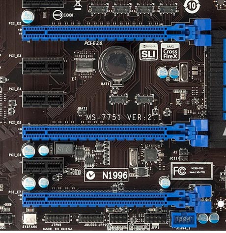
Fig. 2 (PCI-Express 3.0 slots on the motherboard)
Main characteristics of PCI – Express (1.0, 2.0 and 3.0)
Despite the fact that the names PCI and PCI-Express are very similar, the principles of connection (interaction) are fundamentally different. In the case of PCI-Express, a line is used - a bi-directional serial connection, point-to-point, these lines can be several. In the case of video cards and motherboards (we do not take into account Cross Fire and SLI), which support PCI-Express x16 (that is, the majority), you can easily guess that there are 16 such lines (Fig. 3), quite often on motherboards with PCI- E 1.0, you could see a second x8 slot for SLI or Cross Fire.
Well, in PCI, the device connects to a common 32-bit parallel bus.

Rice. 3. An example of slots with different numbers of lines
(as mentioned earlier, x16 is the most commonly used)
For the interface, the bandwidth is 2.5 Gbps. We need this data to track changes in this parameter in different PCI-E versions.
Further, version 1.0 evolved into PCI-E 2.0... As a result of this transformation, we got twice the bandwidth, that is, 5 Gb / s, but I would like to note that the graphics adapters did not particularly benefit in performance, since this is just a version of the interface. Most of the performance depends on the video card itself, the version of the interface can only slightly improve or slow down the data transfer (in this case there is no "braking", and there is a good margin).
In the same way, in 2010, with a margin, the interface was developed PCI-E 3.0, at the moment it is used in all new systems, but if you still have 1.0 or 2.0, then do not worry - below we will talk about the relative backward compatibility of different versions.
In PCI-E 3.0, the bandwidth has been doubled compared to 2.0. Many technical changes were also made there.
Expected to be born by 2015 PCI-E 4.0, which is absolutely not surprising for a dynamic IT industry.
Well, okay, let's finish with these versions and bandwidth numbers, and touch on a very important issue of backward compatibility of various PCI-Express versions.
PCI-Express 1.0, 2.0, and 3.0 backward compatibility
This question worries many, especially when choosing a video card for the current system. Since being content with a system with a motherboard that supports PCI-Express 1.0, doubts arise whether a video card with PCI-Express 2.0 or 3.0 will work correctly? Yes, it will, at least so the developers who have provided this very compatibility promise. The only thing is that the video card will not be able to fully reveal itself in all its glory, but the performance losses, in most cases, will be insignificant.

Quite the opposite, you can safely install video cards with the PCI-E 1.0 interface in motherboards that support PCI-E 3.0 or 2.0, nothing is limited here at all, so be calm about compatibility. If, of course, everything is in order with other factors, these include an insufficiently powerful power supply unit, etc.
In general, we talked in some detail about PCI-Express, which will allow you to get rid of a lot of ambiguities and doubts about compatibility and understanding of differences in PCI-E versions.
The motherboard is the "body" of the computer, and without it no system unit can exist. All components that make up the system unit are attached to the motherboard and connected to it. From the point of view of assembling a computer, connecting elements to the motherboard is not an extremely difficult task, but there are important nuances that you need to pay attention to. In this article, we will consider what are the main connectors on the motherboard, what to connect to them, in which cases they are compatible and in which they are not, as well as other issues.
CPU connector on the motherboard
One of the main components and "heart" of any computer is the central processor. Without it, you will not be able to start the system unit, and it is very important to install it correctly. When choosing a processor, you need to focus on which motherboard is used, or vice versa. The fact is that there are 9 modern processor socket standards that have different pinouts or are not compatible with each other for other reasons.
| CPU |
Connector |
||||
| AMD | AM3 | AM3 + | FM1 | FM2 | |
| Intel | 1150 | 1155 | 1356 | 1366 | 2011 |
The processor socket is usually located in the middle of the motherboard. It is hard not to notice it - it is a large rectangular platform that has a special mechanism for fixing the processor.

Please note: Most of the time around the processor socket on the motherboard is pretty "deserted". The fact is that on top of the processor is installed, which can be quite impressive in size.
Connector for a video card on the motherboard
We recommend reading:The next connector on the motherboard, which is likely to be required when assembling a computer, is the connector for a video card. Some time ago, two types of connectors were used - AGP and PCI Express. Today, all video cards are connected to the PCI Express slot.
Most often, the PCI Express slot is located in the lower left corner of the motherboard. It can serve not only to connect a video card, but also for other devices.

Important: PCI Express slot can be presented in several variations: PCI Express x1, PCI Express x4, PCI Express x16. The last of the listed connectors is used to connect a standard video card. Other connectors may not always be present on modern motherboards.
The PCI Express X16 slot for connecting a video card can be of different versions. As of 2017, there are 4 types of PCI Express slot:
These connectors differ from each other only in bandwidth. However, they are backward compatible.
Example: By plugging a PCI Express 2.0 device into a PCI Express 3.0 slot, it will most likely work flawlessly. But if you do the opposite, then a device designed for a higher type of connector may not have enough bandwidth to fully or partially fulfill its functions.
Worth noting: Some motherboards have a connectorPCI located nearPCIExpress. This connector is now practically not used, but if necessary, additional elements can be installed in it.
RAM connector on the motherboard
We recommend reading:RAM connectors are most often located to the right of the processor (sometimes they can be located on both sides). There are at least 4 such connectors on a modern motherboard.

Currently, the slots for connecting RAM are DDR3 protocol. At the same time, DDR1 and DDR2 were previously used, which lagged behind the modern standard in terms of bandwidth. Connector and device compatibilityDDR1,DDR2 andDDR 3 is not. That is, you will not be able to install a DDR1 device into a DDR3 slot.
It is worth noting: On modern motherboards, you can see that several connectors for connecting RAM are made in one color, and several in another. This is due to the fact that different channels are highlighted in different colors. If you use several strips of RAM, it is better to plug them all into connectors of the same color.
HDD connector on the motherboard
On the motherboard, most often in the lower right part of it, there are several connectors for connecting a hard drive. These connectors are called SATA and they come in three versions: SATA 1.0, SATA 2.0, SATA 3.0. Most often, these connectors are highlighted in color, differing from all other connectors on the motherboard.

All connector versionsSATA are backward compatible and differ in speed. Connector SATA 3.0 is the fastest at the moment, which is why it is used in all modern motherboards.
Motherboard power connector
There is another important connector on the right side of the motherboard that serves to power the motherboard. Usually it consists of 20 or 24 pins and is used to connect to it