Powerful MOSFET field-effect transistors are good for everyone, except for one small nuance - it is often impossible to connect them directly to the pins of the microcontroller.
This is, firstly, due to the fact that permissible currents for microcontroller pins rarely exceed 20 mA, and for very fast switching MOSFETs (with good edges), when you need to very quickly charge or discharge the gate (which always has some capacity) , currents are needed an order of magnitude greater.
And, secondly, the controller’s power supply is usually 3 or 5 Volts, which, in principle, allows direct control only of a small class of field workers (called logic level). And considering that usually the controller’s power supply and the power supply to the rest of the circuit have a common negative wire, this class is reduced exclusively to N-channel “logic level” field devices.
One of the solutions in this situation is the use of special microcircuits - drivers, which are precisely designed to draw large currents through the field gates. However, this option is not without its drawbacks. Firstly, drivers are not always available in stores, and secondly, they are quite expensive.
In this regard, the idea arose to make a simple, low-cost, loose driver that could be used to control both N-channel and P-channel field devices in any low-voltage circuits, say up to 20 volts. Well, fortunately, I, like a real radio junkie, full of all sorts of electronic junk, so after a series of experiments this scheme was born:
- R 1 =2.2 kOhm, R 2 =100 Ohm, R 3 =1.5 kOhm, R 4 =47 Ohm
- D 1 - diode 1N4148 (glass barrel)
- T 1, T 2, T 3 - transistors KST2222A (SOT-23, marking 1P)
- T 4 - transistor BC807 (SOT-23, marking 5C)
The capacitance between Vcc and Out symbolizes the connection of a P-channel field switch, the capacitance between Out and Gnd symbolizes the connection of an N-channel field switch (the gate capacitance of these field switches).
The dotted line divides the circuit into two stages (I and II). In this case, the first stage works as a power amplifier, and the second stage as a current amplifier. The operation of the circuit is described in detail below.
So. If a high signal level appears at the In input, then the transistor T1 opens, the transistor T2 closes (since the potential at its base drops below the potential at the emitter). As a result, transistor T3 closes, and transistor T4 opens and through it the gate capacitance of the connected field switch is recharged. (The base current of transistor T4 flows along the path E T4 -> B T4 -> D1-> T1-> R2-> Gnd).
If a low signal level appears at the In input, then everything happens the other way around - transistor T1 closes, as a result of which the base potential of transistor T2 increases and it opens. This in turn causes transistor T3 to turn on and transistor T4 to turn off. The gate capacitance of the connected field switch is recharged through the open transistor T3. (The base current of transistor T3 flows along the path Vcc->T2->R4->B T3 ->E T3).
That's basically the whole description, but some points probably require additional explanation.
First, what are transistor T2 and diode D1 in the first stage? Everything is very simple here. It’s not for nothing that I wrote above the paths of the base currents of the output transistors for different states of the circuit. Look at them again and imagine what would happen if there were no transistor T2 with the harness. In this case, transistor T4 would be unlocked by a large current (meaning the base current of the transistor) flowing from the Out output through open T1 and R2, and transistor T3 would be unlocked by a small current flowing through resistor R3. This would result in a very long leading edge of the output pulses.
Well, secondly, many will probably be interested in why resistors R2 and R4 are needed. I plugged them in in order to at least slightly limit the peak current through the bases of the output transistors, as well as to finally equalize the leading and trailing edges of the pulses.
The assembled device looks like this:
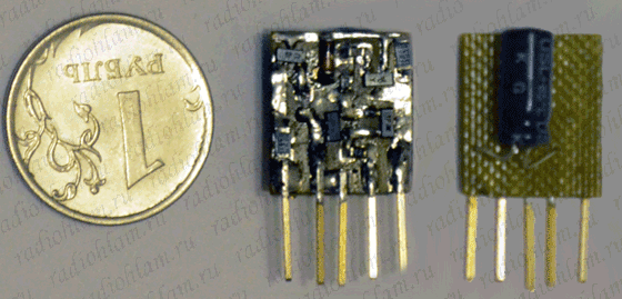
The driver layout is made for SMD components, and in such a way that it can be easily connected to the main board of the device (in a vertical position). That is, we can have a half-bridge or something else installed on the main board, and all that remains is to vertically plug the driver boards into this board in the right places.
The wiring has some peculiarities. To radically reduce the size of the board, we had to “slightly incorrectly” route the T4 transistor. Before soldering it to the board, you need to turn it face down (marked) and bend the legs in the opposite direction (toward the board).
As you can see, the duration of the fronts is practically independent of the supply voltage level and is slightly more than 100 ns. In my opinion, pretty good for such a budget design.
Perhaps after reading this article you will not have to install radiators of the same size on transistors.
Translation of this article.
A short message from the translator:
Firstly, in this translation there may be serious problems with the translation of terms, I have not studied electrical engineering and circuit design enough, but I still know something; I also tried to translate everything as clearly as possible, so I did not use concepts such as bootstrap, MOSFET, etc. Secondly, if it is now difficult to make a spelling mistake (praise be to word processors for indicating errors), then it is quite easy to make a mistake in punctuation.
And on these two points, I ask you to kick me in the comments as hard as possible.
Now let's talk more about the topic of the article - with all the variety of articles about building various ground-based vehicles (cars) on MK, on Arduino, on<вставить название>, the design of the circuit itself, much less the motor connection circuit, is not described in sufficient detail. It usually looks like this:
- take the engine
- take the components
- connect the components and the engine
- …
- PROFIT!1!
But to build more complex circuits than simply turning a PWM motor in one direction through L239x, you usually need knowledge about full bridges (or H-bridges), about field-effect transistors (or MOSFETs), and about drivers for them. If there are no restrictions, then you can use p-channel and n-channel transistors for a full bridge, but if the engine is powerful enough, then the p-channel transistors will first have to be hung with a large number of radiators, then coolers will be added, but if it’s a shame to throw them out completely, then you can try other types of cooling, or simply use only n-channel transistors in the circuit. But there is a small problem with n-channel transistors - it can sometimes be quite difficult to open them “in an amicable way”.
So I was looking for something to help me with making a proper diagram and I found an article on the blog of a young man named Syed Tahmid Mahbub. I decided to share this article.
In many situations we must use FETs as high-level switches. Also in many situations we must use field-effect transistors as switches for both the upper and lower levels. For example, in bridge circuits. In partial bridge circuits we have 1 high level MOSFET and 1 low level MOSFET. In full bridge circuits we have 2 high level MOSFETs and 2 low level MOSFETs. In such situations, we will need to use both high and low level drivers together. The most common way to control field-effect transistors in such cases is to use a low- and high-level switch driver for MOSFETs. Undoubtedly, the most popular driver chip is the IR2110. And in this article/textbook I will talk about exactly that.
You can download documentation for the IR2110 from the IR website. Here is the download link: http://www.irf.com/product-info/datasheets/data/ir2110.pdf
Let's first take a look at the block diagram, as well as the description and location of the pins:

Figure 1 - Functional block diagram of IR2110

Figure 2 - IR2110 pinout

Figure 3 - Description of IR2110 pins
It's also worth mentioning that the IR2110 comes in two packages - a 14-pin PDIP pinout and a 16-pin SOIC surface mount.
Now let's talk about various contacts.
VCC is the low level power supply, should be between 10V and 20V. VDD is the logic supply for the IR2110, it should be between +3V and +20V (relative to VSS). The actual voltage you choose to use depends on the voltage level of the input signals. Here's the chart:

Figure 4 - Dependence of logic 1 on power
Typically a VDD of +5V is used. When VDD = +5V, the input threshold of logic 1 is slightly higher than 3V. Thus, when VDD = +5V, IR2110 can be used to control the load when input “1” is higher than 3 (some) volts. This means that the IR2110 can be used for almost all circuits, since most circuits tend to be powered at around 5V. When you use microcontrollers, the output voltage will be higher than 4V (after all, the microcontroller quite often has VDD = +5V). When using an SG3525 or TL494 or other PWM controller, you will probably have to power them with a voltage greater than 10V, which means the outputs will be greater than 8V at logic one. Thus, the IR2110 can be used almost anywhere.
You can also reduce the VDD to around +4V if you are using a microcontroller or any chip that outputs 3.3V (eg dsPIC33). When designing circuits with the IR2110, I noticed that sometimes the circuit did not work properly when the VDD of the IR2110 was set to less than +4V. Therefore, I do not recommend using VDD below +4V. In most of my circuits the signal levels do not have a voltage less than 4V as a "1" and so I use VDD = +5V.
If for some reason in the circuit the level of the logical “1” signal has a voltage less than 3V, then you need to use a level converter/level translator, it will raise the voltage to acceptable limits. In such situations, I recommend increasing to 4V or 5V and using the IR2110 VDD = +5V.
Now let's talk about VSS and COM. VSS is the land for logic. COM is "low level return" - basically the driver's low level ground. It may look like they are independent, and one might think that it would perhaps be possible to isolate the driver outputs and the driver signal logic. However, this would be wrong. Although they are not internally coupled, the IR2110 is a non-isolated driver, meaning that VSS and COM must both be connected to ground.
HIN and LIN are logical inputs. A high signal on HIN means that we want to control the high key, that is, high level output is carried out on HO. A low signal on HIN means we want to turn off the high level MOSFET, that is, HO is the low level output. The output to HO, high or low, is not considered relative to ground, but relative to VS. We will soon see how the amplifier circuits (diode + capacitor) using VCC, VB and VS provide floating power to drive the MOSFET. VS is floating power return. At high level, the level at HO is equal to the level at VB, relative to VS. At low level, the level at HO is equal to VS, relative to VS, effectively zero.
A high LIN signal means that we want to control the low switch, that is, LO outputs a high level. A low LIN signal means we want to turn off the low level MOSFET, that is, LO is the low level output. The output in LO is considered relative to ground. When the signal is high, the level at LO is the same as at VCC, relative to VSS, effectively ground. When the signal is low, the level in LO is the same as in VSS, relative to VSS, effectively zero.
SD is used as stop control. When the level is low, IR2110 is on - the stop function is disabled. When this pin is high, the outputs are turned off, disabling control of the IR2110.
Now let's take a look at a common configuration with the IR2110 to drive MOSFETs as high and low switches - half bridge circuits.

Figure 5 - Basic circuit on IR2110 for half-bridge control
D1, C1 and C2 together with IR2110 form the amplifier circuit. When LIN = 1 and Q2 is turned on, C1 and C2 are charged to VB level, since one diode is located below +VCC. When LIN = 0 and HIN = 1, the charge on C1 and C2 is used to add additional voltage, VB in this case, above the Q1 source level to drive Q1 in a high switch configuration. A sufficiently large capacitance must be selected at C1 so that it is enough to provide the necessary charge to Q1 so that Q1 is turned on the entire time. C1 should also not have too much capacitance, since the charging process will take a long time and the voltage level will not increase enough to keep the MOSFET turned on. The longer the time required in the on state, the larger the capacity required. Thus, a lower frequency requires a larger capacitance C1. A higher fill factor requires a larger capacitance C1. Of course, there are formulas for calculating capacitance, but for this you need to know many parameters, and we may not know some of them, for example, the leakage current of a capacitor. So I just estimated the approximate capacity. For low frequencies such as 50Hz, I use a capacitance of 47uF to 68uF. For high frequencies such as 30-50kHz, I use capacitances ranging from 4.7uF to 22uF. Since we are using an electrolytic capacitor, a ceramic capacitor must be used in parallel with this capacitor. A ceramic capacitor is not necessary if the boost capacitor is tantalum.
D2 and D3 discharge the gate of the MOSFETs quickly, bypassing the gate resistors and reducing turn-off time. R1 and R2 are current limiting gate resistors.
MOSV can be maximum 500V.
VCC should come from the source without interference. You must install filtering and decoupling capacitors from +VCC to ground for filtering.
Let's now look at some example circuits with IR2110.

Figure 6 - Circuit with IR2110 for high voltage half bridge

Figure 7 - Circuit with IR2110 for a high-voltage full bridge with independent key control (clickable)
In Figure 7 we see the IR2110 used to control a full bridge. There is nothing complicated about it and I think you already understand this. You can also apply a fairly popular simplification here: we connect HIN1 to LIN2, and we connect HIN2 to LIN1, thus we get control of all 4 keys using only 2 input signals, instead of 4, this is shown in Figure 8.

Figure 8 - Scheme with IR2110 for a high-voltage full bridge with key control with two inputs (clickable)

Figure 9 - Circuit with IR2110 as a high-voltage top-level driver
In Figure 9 we see the IR2110 used as a high-level driver. The circuit is quite simple and has the same functionality as described above. One thing that needs to be taken into account is that since we no longer have a low level switch, there must be a load connected from OUT to ground. Otherwise, the amplifier capacitor will not be able to charge.

Figure 10 - Circuit with IR2110 as a low-level driver

Figure 11 - Circuit with IR2110 as a dual low-level driver
If you're having problems with your IR2110 and everything keeps failing, burning, or exploding, I'm pretty sure it's because you're not using gate-source resistors, assuming you designed it carefully, of course. NEVER FORGET ABOUT GATE-SOURCE RESISTORS. If you're interested, you can read about my experience with them here (I also explain the reason why resistors prevent damage).
2.3. Drivers for controlling powerful transistors
Drivers are control chips that connect various controllers and logic circuits with powerful transistors in the output stages of converters or motor control devices. Drivers, providing signal transmission, must introduce as little time delay as possible, and their output stages must withstand the large capacitive load characteristic of the gate circuits of transistors. The sink and sink currents of the driver output stage should be between 0.5 and 2 A or more.
The driver is a pulse power amplifier and is designed to directly control the power switches of power parameter converters. The driver circuit is determined by the type of structure of the key transistor (bipolar, MOS or IGBT) and the type of its conductivity, as well as the location of the transistor in the switch circuit (“upper”, i.e. one whose both power terminals in the open state have a high potential, or “ lower", both power terminals of which in the open state have zero potential). The driver must amplify the control signal in terms of power and voltage, and, if necessary, provide its potential shift. The driver can also be assigned key protection functions.
When designing a control circuit for power transistor assemblies, you need to know that:
a) it is necessary to provide a “floating” potential for controlling the “upper” power switch in the semi-bridge circuit;
b) it is extremely important to create a rapid rise and fall of control signals arriving at the gates of power elements to reduce switching heat losses;
c) it is necessary to ensure a high value of the gate control current pulse of the power elements to quickly recharge the input capacitors;
d) in the vast majority of cases, electrical compatibility of the driver input part with standard TTL/CMOS digital signals (usually coming from microcontrollers) is required.
For quite a long time, developers were forced to design control driver circuits using discrete elements. The first important event on the path of integration of control drivers was the appearance of microcircuits of the IR21xx and IR22xx series (and then their more modern modifications IRS21xx, IRS22xx), developed by International Rectifies. These microcircuits today have found wide application in low-power converter technology, since they meet all the above requirements.
The power switch control circuit is always constructed in such a way that its output signal (in the form of width-modulated pulses) is specified relative to the “common” conductor of the circuit. As can be seen from Fig. 2.12, A, which shows a semi-bridge power stage for a switching transistor VT 2 this is quite enough - the signal “Control 2” can be directly applied to the gate (base) of the transistor through the driver G2, since its source (emitter) is connected to the “common” conductor of the circuit, and control is carried out relative to the “common” conductor.
But what about the transistor? VT 1, which operates in the upper arm of the half-bridge? If the transistor VT 2 is in the closed state, and VT 1 open, at source VT 1 supply voltage present E Pete. Therefore, to switch the transistor VT 1, you need a device G1 galvanically isolated from the “common” circuit, which will clearly transmit the pulses of the control circuit “Control 1” without introducing distortion into the signals. The classic solution to this problem is to turn on the control transformer T1 (Fig. 2.12, b), which, on the one hand, galvanically isolates the control circuits, and on the other hand, transmits switching pulses. It is no coincidence that this technical solution is considered a “classic of the genre”: it has been known for decades.
A b
Rice. 2.12. Power switches in half-bridge circuits
The input signal is a control chip signal of standard logic level amplitude, and using the voltage applied to the Vdd pin, compatibility with classic 5-volt “logic” and more modern 3.3-volt logic can be achieved. At the driver output there are control voltages for the “upper” and “lower” power transistors. The driver has taken measures to ensure the necessary control levels, an equivalent of galvanic isolation (pseudo-isolation) has been created, and there are additional functions - a shutdown input, an undervoltage protection unit, and a short control pulse filter.
As can be seen from the block diagram (Fig. 2.13), the driver consists of two independent channels, which are designed to control the upper and lower arms of half-bridge circuits. At the driver input there are pulse shapers built on the basis of Schmitt triggers. The Vcc and Vdd inputs are intended for connecting the supply voltage to the power and control parts of the circuit, the “ground” buses of the power part and the control part are decoupled (different “common” terminals - Vss and COM).
In the vast majority of cases, these pins are simply connected together. There is also the possibility of separate power supply of the control and power parts to match the input levels with the levels of the control circuit. SD input is protective. The output stages are built on complementary field-effect transistors. The microcircuit contains additional devices that ensure its stable operation as part of conversion circuits: this is a device for shifting the level of control signals (Vdd/Vcc level shift), a device for suppressing short impulse noise (pulse filter), a switching delay device (delay) and an undervoltage detector power supply (UV detect).

Rice. 2. 13. Functional units of the IRS2110 and IRS2113 microcircuits
A typical driver connection diagram is shown in Fig. 2.14. Capacitors WITH 1 and WITH Z - filtering. The manufacturer recommends placing them as close as possible to the corresponding terminals. Capacitor WITH 2 and diode VD 1 - bootstrap stage, which provides power to the control circuit of the “upper” side transistor. Capacitor WITH 4 - filter in the power circuit. Resistors R 1 and R 2 - shutter.
Sometimes the width-modulated control signal can be generated not at two control inputs separately, but rather applied to one input in the form of a meander with a varying duty cycle. This control method can be found, for example, in converters that generate a sinusoidal signal of a given frequency. In this case, it is enough to set a “dead time” pause between the closing of one half-bridge transistor and the opening of the second.

Rice. 2.14. Typical connection diagram for IRS2110 and IRS2113
Such a driver with a built-in unit for guaranteed formation of a “dead time” pause is available in the International Rectifies product range - this is the IRS2111 microcircuit (Fig. 2.15).

Rice. 2.15. Functional components of the IRS2111 chip
The block diagram shows that the driver has built-in units for forming a “dead time” pause for the upper and lower arms of the half-bridge. According to the manufacturer’s documentation, the “dead time” value is set at 650 ns (typical value), which is quite enough to control half-bridges consisting of power MOSFET transistors.
Drivers for controlling complex converter circuits - single-phase and three-phase - contain a large number of elements, so it is not surprising that they are produced in the form of integrated circuits. These microcircuits, in addition to the drivers themselves, also contain level conversion circuits, auxiliary logic, delay circuits for the formation of “dead” time, protection circuits, etc. Based on the scope of application of IC drivers, they are distinguished: low key drivers; top key drivers; lower and upper key drivers; half-bridge drivers; single-phase bridge drivers; three-phase bridge drivers.
The main parameters of integrated drivers are divided into two groups: dynamic and operational. Dynamic ones include the switching delay time when unlocking and locking the key, the rise and fall time of the output voltage, as well as the reaction time of the protection circuits. The most important operational parameters: maximum pulse value of the incoming/outgoing output current, input levels, supply voltage range, output resistance.
Drivers are often also assigned some protection functions for MOS and JGVT transistors. These features include: key short circuit protection; driver undervoltage protection;
protection against through currents; protection against gate breakdown.
Questions for self-control
What are the main differences between bipolar and field-effect transistors that should be taken into account when using them as electronic switches?
What advantages of bipolar and field-effect transistors does MOPBT combine?
List the main static operating modes of transistors. In what modes should transistors be used in power electronics devices?
Using the Larionov scheme, explain the essence of pulse width
modulation (PWM).
Power transistors IGBT and MOSFET have become the main elements used in high-power switching converters. Their unique static and dynamic characteristics make it possible to create devices capable of delivering tens and even hundreds of kilowatts to the load with minimal dimensions and an efficiency exceeding 95%.
What IGBTs and MOSFETs have in common is an insulated gate, resulting in similar drive characteristics. Thanks to the negative temperature coefficient of short-circuit current, it became possible to create short-circuit-resistant transistors. Now transistors with a standardized overcurrent time are produced by almost all leading companies.
The absence of control current in static modes makes it possible to abandon control circuits based on discrete elements and create integrated control circuits - drivers. Currently, a number of companies, such as International Rectifier, Hewlett-Packard, Motorola, produce a wide range of devices that control single transistors, half-bridges and bridges - two- and three-phase. In addition to providing gate current, they are also capable of performing a number of auxiliary functions, such as overcurrent and short circuit protection ( Overcurrent Protection, Short Circuit Protection) and control voltage drop ( Under Voltage LockOut- UVLO). For key elements with a control gate, a drop in control voltage is a dangerous condition. In this case, the transistor can go into linear mode and fail due to overheating of the crystal.
It can be difficult for users to understand the wide range of microcircuits currently produced for use in power circuits, despite the similarity of their basic characteristics. This article discusses the features of using the most popular drivers produced by various companies.
The main auxiliary function of the drivers is overcurrent protection. To better understand the operation of the protection circuit, it is necessary to analyze the behavior of power transistors in short circuit mode (or short circuit - an abbreviation familiar to developers).
The causes of current overloads are varied. Most often these are emergency cases, such as a breakdown on the housing or a load short circuit.
Overload can also be caused by circuit features, such as transients or reverse recovery current of the opposed-side diode. Such overloads must be eliminated by circuit engineering methods: the use of trajectory shaping circuits (snubbers), the choice of a gate resistor, the isolation of control circuits from power buses, etc.
Turning on the transistor during a short circuit in the load circuit
The schematic diagram and voltage diagrams corresponding to this mode are shown in Fig. 1 a and 2. All graphs were obtained by analyzing the circuits using the PSpice program. For the analysis, improved models of MOSFET transistors from International Rectifier and macromodels of IGBTs and drivers developed by the author of the article were used.

Rice. 2
Short circuit of the load at the switched on transistor

Rice. 3
As noted, the steady-state value of the short-circuit current is determined by the voltage at the gate. However, reducing this voltage leads to an increase in the saturation voltage and, consequently, to an increase in conduction losses. Short circuit resistance is closely related to the transistor transconductance. High current gain IGBTs have a low saturation voltage but a short overload time. As a rule, transistors that are most resistant to short circuits have a high saturation voltage and, therefore, high losses.
The permissible short-circuit current of an IGBT is much higher than that of a bipolar transistor. It is typically equal to 10 times the rated current at the permissible gate voltages. Leading companies, such as International Rectifier, Siemens, Fuji, produce transistors that can withstand such overloads without damage. This parameter is specified in the reference data for transistors and is called Short Circuit Ration, and the permissible overload time is tsc - Short Circuit Withstand Time.
The fast response of the protection circuit is generally useful for most applications. The use of such circuits in combination with highly cost-effective IGBTs increases the efficiency of the circuit without compromising reliability.
Using drivers to protect against overloads
Let's consider methods for turning off transistors in overload mode using the example of drivers manufactured by International Rectifier, Motorola and Hewlett-Packard, since these microcircuits allow you to implement protection functions most fully.
Upper arm driver

Rice. 4. IR2125 driver structure
In Fig. 4 shows a block diagram, and Fig. 5 - typical connection diagram for the IR2125 driver using the overload protection function. Pin 6 - CS is used for this purpose. The protection response voltage is 230 mV. To measure the current, a resistor RSENSE is installed in the emitter, the value of which and the divider R1, R4 determine the protection current.

Rice. 5. Connection diagram IR2125
As mentioned above, if the gate voltage is reduced when an overload occurs, the emergency mode recognition period can be increased. This is necessary to exclude false positives. This function is implemented in the IR2125 chip. Capacitor C1 connected to the ERR pin determines the analysis time for the overload condition. At C1 = 300 pF, the analysis time is about 10 μs (this is the time it takes to charge the capacitor to a voltage of 1.8 V - the threshold voltage of the circuit comparator ERROR TIMING driver). During this time, the collector current stabilization circuit is turned on, and the gate voltage decreases. If the overload condition does not stop, then after 10 μs the transistor turns off completely.
The protection is turned off when the input signal is removed, which allows the user to organize a trigger protection circuit. When using it, special attention should be paid to the selection of the restart time, which should be greater than the thermal time constant of the power transistor crystal. The thermal time constant can be determined from a plot of the thermal impedance Zthjc for single pulses.

Rice. 6
A measuring resistor is not required to analyze saturation voltage overload conditions. When a positive control signal is applied to the gate, a voltage appears at the SC driver protection input, determined by the sum of the voltage drop across the open diode VD2 and the open power transistor Q1 and the divider R1, R4, which sets the operating current. The voltage drop across the diode is almost constant and is about 0.5 V. The open transistor voltage at the selected short circuit current is determined from the graph Von = f(Ic). Diode VD4, like VD1, must be fast and high voltage.
In addition to overcurrent protection, the driver analyzes the supply voltage of the input part VCC and the output stage VB, turning off the transistor when VB drops below 9 V, which is necessary to prevent linear operation of the transistor. This situation can arise either if the low-voltage power supply is damaged or if capacitance C2 is chosen incorrectly. The value of the latter must be calculated based on the values of the gate charge, gate current and pulse repetition rate. To calculate the bootstrap capacity Cb, the International Rectifier documentation recommends the following formulas:
Cb = 15*2*(2*Qg + Igbs/f + It)/(Vcc – Vf – Vls),
It = (Ion + Ioff)*tw.
Where
Ion and Ioff - gate on and off currents, tw = Qg/Ion - switching time, Qg - gate charge, f - pulse repetition rate, Vcc - supply voltage, Vf - forward voltage drop across the charge pump diode (VD1 in Fig. 6 ), Vls is the forward voltage drop across the opposed diode (VD3 in Fig. 6), Igbs is the gate current in static mode.
If it is impossible to power the driver from the bootstrap capacity, it is necessary to use a “floating” power source.
Three-phase bridge driver
In Fig. Figure 7 shows the connection diagram for the IR213* three-phase bridge driver using the overload protection function. The ITR input is used for this purpose. The protection response voltage is 500 mV. To measure the total bridge current, a resistor RSENSE is installed in the emitters, the value of which, together with the divider R2, R3, determines the protection current.

Rice. 7. Connection diagram for IR2130
The IR2130 driver provides control of MOSFET and IGBT transistors at voltages up to 600 V, has protection against overcurrent and reduction in supply voltages. The protection circuit contains an open-drain field-effect transistor to indicate a fault (FAULT). It also has a built-in load current amplifier, which allows the generation of control and feedback signals. The driver generates the delay time (tdt - deadtime) between turning on the upper and lower side transistors to eliminate through currents. This time ranges from 0.2 to 2 μs for various modifications.
To properly use this microcircuit and create reliable circuits based on it, several nuances must be taken into account.
A feature of the IR213* drivers is the absence of a gate voltage limiting function during a short circuit. For this reason, the time constant of the R1C1 chain, designed to delay the activation of the protection, should not exceed 1 μs. The designer should be aware that the bridge will turn off 1 µs after the fault occurs, as a result of which the current (especially with a resistive load) may exceed the rated value. To reset the protection, you must turn off the driver power or apply a blocking voltage (high level) to the low-level inputs. We also note that among the microcircuits of this series there is an IR2137 driver, which provides protection for the saturation voltage of the upper transistors and generates the required delay time for the operation of this protection. Such protection is very important for drivers that control three-phase bridge circuits, since when a breakdown occurs on the housing, the short-circuit current flows bypassing the RSENSE measuring resistor. This microcircuit provides separate connection of gate resistors for on, off and emergency shutdown, which allows you to fully realize all the dynamic features of insulated gate transistors.
The on/off current for IR213* is 200/420 mA (120/250 mA for IR2136). This must be taken into account when choosing power transistors and gate resistors for them. The parameters for the transistor indicate the amount of gate charge (usually in nK), which determines the on/off time of the transistor at a given current. The duration of transient processes associated with switching must be less than the delay time tdt generated by the driver. The use of high-power transistors can also lead to false on-off and through-current due to the Miller effect. Reducing the gate resistor or using separate gate resistors for the turn-on and turn-off processes does not always solve the problem due to insufficient turn-off current from the driver itself. In this case, it is necessary to use buffer amplifiers.
The advantage of chips manufactured by International Rectifier is that these devices are able to withstand high voltage differences between the input and output parts. For IR21** series drivers, this voltage is 500–600 V, which allows you to control transistors in half-bridge and bridge circuits when powered by a rectified industrial voltage of 220 V without galvanic isolation. To control transistors in circuits designed for power supply from a rectified voltage of 380 V, International Rectifier produces drivers of the IR22 series**. These microcircuits operate at output voltages up to 1200 V. All International Rectifier drivers can withstand induced voltage rises up to 50 V/ns. This parameter is called dv/dt immune. It demonstrates high resistance to latch-up mode, which is extremely dangerous for pulsed high-voltage circuits.
Low arm driver
To control low-side transistors, microcircuits manufactured by Motorola provide a good alternative. The block diagram of one of them - MC33153 is shown in Fig. 8.

Rice. 8. Block diagram of MC33153
A feature of this driver is the ability to use two methods of protection (current and saturation voltage) and the separation of overload mode and short circuit mode. It is also possible to supply negative control voltage, which can be very useful for driving high-power modules with high gate charge values. Control voltage drop shutdown - UVLO is carried out at 11 V.
Output 1 ( Current Sense Input) is intended for connecting a current measuring resistor. In the microcircuit, this pin is the input of two comparators - with an operating voltage of 65 and 130 mV. Thus, the driver analyzes the overload and short circuit conditions. When overload occurs, the first comparator is triggered ( Overcurrent Comparator) and turns off the gate control signal. The protection is reset when a blocking signal is applied (high level, since the Input input is inverting). In this case, a fault signal is output ( Fault Output) is not served. If the current exceeds the specified value twice, this is regarded as a short circuit. In this case, the second comparator is overturned ( Short Circuit Comparator), and a high level signal appears at the control output. Based on this signal, the controller that controls the operation of the circuit must turn off the entire circuit. The restart time should be determined, as mentioned above, by the thermal time constant of the power transistors.
Output 8 ( Desaturation Input) is designed to implement saturation voltage protection. The response voltage at this input is 6.5 V. The same input is intended for connecting a capacitor Cblank, which forms the protection response delay time. This delay is necessary because after the gate voltage is applied to the gate, the transistor maintains a high voltage for some time while the boxer diode is recovering.

Rice. 9. Saturation voltage protection

Rice. 10. Current protection
Driver with galvanic isolation
Galvanic isolation is necessary in circuits where a powerful power stage is powered from the mains voltage, and control signals are generated by a controller connected via buses to various peripheral devices. Isolating the power and control circuitry in such cases reduces switching noise and allows low-voltage circuits to be protected in extreme cases.

Rice. 11. Block diagram of HCPL316
In our opinion, one of the most interesting microcircuits for this application is the HCPL316 manufactured by Hewlett-Packard. Its structure is shown in Fig. 11, and the connection diagram is in Fig. 12.

Rice. 12. Connection diagram HCPL316
The control signal and the fault signal are optically isolated. The insulation voltage is up to 1500 V. The driver provides protection only for saturation voltage (pin 14 - DESAT). An interesting feature is the presence of direct and inverse input, which simplifies communication with various types of controllers. As in the case of MC33153, the microcircuit can produce a bipolar output signal, and the peak output current can reach 3 A. Thanks to this, the driver is able to drive IGBT transistors with a collector current of up to 150 A, which is its big advantage compared to similar devices.
Auxiliary circuits
In high-voltage drivers from International Rectifier, due to their low consumption, the output stages can be powered using so-called “bootstrap” capacitors of small values. If this is not possible, it is necessary to use “floating” power supplies. The cheapest way to use such sources is multi-winding transformers with a rectifier and stabilizer on each winding. Naturally, if you want to have a bipolar output signal, then each such source must be bipolar. However, a more elegant solution is to use isolated DC-DC converters, such as the DCP01* series from Burr-Brown. These microcircuits are designed for power up to 1W and can generate a bipolar output signal from a unipolar input signal. Isolation voltage is up to 1 kV. Isolation is carried out using a transformer barrier at a frequency of 800 kHz. When using several chips, they can be synchronized in frequency.
In power drives it is often necessary to have a signal proportional to the output current to generate feedback. This problem is solved in different ways: using current transformers, shunts and differential amplifiers, etc. All these methods have their drawbacks. To most successfully solve the problem of generating a current signal and connecting it with the controller, International Rectifier has developed microcircuits - current sensors IR2171 and IR2172, in which the current signal is converted into a PWM signal. The connection diagram for IR2171 is shown in Fig. 13. The microcircuit can withstand voltage drops of up to 600 V and is powered by a “bootstrap” capacitance. The PWM carrier frequency is 35 kHz for IR2171 and 40 kHz for IR2172. Input voltage range ±300 mV. The output voltage is taken from the open collector, which makes it easy to connect optical isolation.
It is hardly possible to describe all the microcircuits currently produced in the world for use in power drives. However, even the information provided should help the developer navigate the ocean of modern element base. The main conclusion from all that has been said is the following: do not try to make something using discrete elements until you are sure that no one is producing an integrated circuit that solves your problem.
Literature
- Use Gate Charge to Design the Gate Drive Circuit for Power MOSFETs and IGBTs. AN-944.
- Application Characterization of IGBTs. INT990.
- IGBT Characteristics. AN-983.
- Short Circuit Protection. AN-984.
- HV Floating MOS-Gate Driver Ics. AN-978.
- Motorola MC33153 Technical Data.
- Hewlett Packard HCPL316 Technical Data.
- Burr Brown DCP011515 Technical Data.
- Ivanov V.V., Kolpakov A. Application of IGBT. Electronic components, 1996, No. 1.
MOP (in bourgeois MOSFET) stands for Metal-Oxide-Semiconductor, from this abbreviation the structure of this transistor becomes clear.
If on the fingers, then it has a semiconductor channel that serves as one plate of the capacitor and the second plate is a metal electrode located through a thin layer of silicon oxide, which is a dielectric. When voltage is applied to the gate, this capacitor is charged, and the electric field of the gate pulls charges to the channel, as a result of which mobile charges appear in the channel that can form an electric current and the drain-source resistance drops sharply. The higher the voltage, the more charges and lower the resistance, as a result, the resistance can drop to tiny values - hundredths of an ohm, and if you raise the voltage further, a breakdown of the oxide layer and the Khan transistor will occur.
The advantage of such a transistor, compared to a bipolar one, is obvious - voltage must be applied to the gate, but since it is a dielectric, the current will be zero, which means the required the power to control this transistor will be scanty, in fact, it only consumes at the moment of switching, when the capacitor is charging and discharging.
The disadvantage arises from its capacitive property - the presence of capacitance on the gate requires a large charging current when opening. In theory, equal to infinity on infinitely small periods of time. And if the current is limited by a resistor, then the capacitor will charge slowly - there is no escape from the time constant of the RC circuit.
MOS transistors are P and N duct. They have the same principle, the only difference is the polarity of the current carriers in the channel. Accordingly, in different directions of the control voltage and inclusion in the circuit. Very often transistors are made in the form of complementary pairs. That is, there are two models with exactly the same characteristics, but one of them is N channel, and the other is P channel. Their markings, as a rule, differ by one digit.
 |
My most popular MOP transistors are IRF630(n channel) and IRF9630(p channel) at one time I made about a dozen of them of each type. Possessing a not very large body TO-92 this transistor can famously pull through itself up to 9A. Its open resistance is only 0.35 Ohm.
However, this is a fairly old transistor; now there are cooler things, for example IRF7314, capable of carrying the same 9A, but at the same time it fits into an SO8 case - the size of a notebook square.
One of the docking problems MOSFET transistor and microcontroller (or digital circuit) is that in order to fully open until completely saturated, this transistor needs to drive quite a bit more voltage onto the gate. Usually this is about 10 volts, and the MK can output a maximum of 5.
There are three options:
 But in general, it is more correct to install a driver, because in addition to the main functions of generating control signals, it also provides current protection, protection against breakdown, overvoltage, as an additional bauble, optimizes the opening speed to the maximum, in general, it does not consume its current in vain.
 Choosing a transistor is also not very difficult, especially if you don’t bother with limiting modes. First of all, you should be concerned about the value of the drain current - I Drain or I D you choose a transistor based on the maximum current for your load, preferably with a margin of 10 percent. The next important parameter for you is VGS- Source-Gate saturation voltage or, more simply, control voltage. Sometimes it is written, but more often you have to look at the charts. Looking for a graph of the output characteristic Dependency I D from VDS at different values VGS. And you figure out what kind of regime you will have.
For example, you need to power the engine at 12 volts, with a current of 8A. You screwed up the driver and only have a 5 volt control signal. The first thing that came to mind after this article was IRF630. The current is suitable with a margin of 9A versus the required 8. But let’s look at the output characteristic:
If you are going to use PWM on this switch, then you need to inquire about the opening and closing times of the transistor, choose the largest one and, relative to the time, calculate the maximum frequency of which it is capable. This quantity is called Switch Delay or t on,t off, in general, something like this. Well, the frequency is 1/t. It’s also a good idea to look at the gate capacity C iss Based on it, as well as the limiting resistor in the gate circuit, you can calculate the charging time constant of the RC gate circuit and estimate the performance. If the time constant is greater than the PWM period, then the transistor will not open/close, but will hang in some intermediate state, since the voltage at its gate will be integrated by this RC circuit into a constant voltage.
When handling these transistors, keep in mind the fact that They are not just afraid of static electricity, but VERY STRONG. It is more than possible to penetrate the shutter with a static charge. So how did I buy it? immediately into foil and don’t take it out until you seal it. First ground yourself to the battery and put on a foil hat :).