Sent by:
Simple schemes are not always worse than sophisticated ones. And circuits based on discrete elements are in no way inferior to ready-made microcircuits. Another example can be seen here.
One of the most popular electronic devices nowadays are low-power single-cycle DC-DC converters, widely used in portable battery equipment. Naturally, many companies are actively developing in this area, and there are countless such ready-made devices. In Fig. As an example, Figure 1 shows a block diagram of one of the common TPS61045 converters manufactured by Texas Instruments.

This block diagram is not anything outstanding in terms of the number of elements used, no less than those in similar devices from other manufacturers. This is probably why integrated DC-DC converters are quite expensive electronic products. In addition to the exaggerated block diagram, some of these devices suffer from impulse instability due to an unreasonably large conversion coefficient in the OOS loop. For example, in Fig. Figure 2 shows a simplified voltage waveform in this mode across the inductance of the SP6641 converter from Sipex.

Apparently, the above facts were a consequence of the use of integrated technologies, which, having eliminated the direct relationship between the number of components used and the size of electronic devices, at the same time eliminated the motivation to create optimal electronics. As a result, the unnecessary complexity of integrated circuits has become widespread, and consumers have to pay for it.
Therefore, this article makes an attempt to show that if you do not use unnecessary components to implement electronic devices, then you get products that are in no way inferior to integrated analogues, and in some respects even superior to them. Starting at a lower cost.
In addition, since such devices contain exactly as many components as is necessary to solve a specific problem, they are almost as good as integrated analogues in terms of the area they occupy on the board, although they are made on separate elements. Moreover, implementation on individual elements often makes it possible to provide better electrical parameters than integrated circuits, since the developer has the opportunity to select the best discrete components at the moment when creating his device, which cannot be ensured when using ready-made microcircuits, the quality of the elements used in which is forever tied to period of their development.
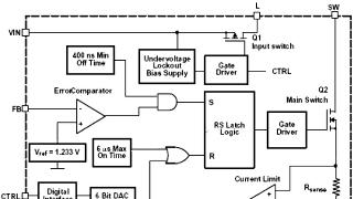
The electrical circuit of a single-cycle converter, confirming the above, is presented in Fig. 3.

The structure of the presented device is universal and allows you to create converters with any type of modulation.
In this case, pulse-frequency modulation is used, which not only makes it possible to implement the simplest structure of the converter, but also contributes to its higher efficiency compared to converters using PWM. This is explained by the fact that when using pulse-frequency modulation and reducing the current in the load, the efficiency decreases only due to the initial current consumption of the output switch control circuit, in contrast to converters with PWM, where the efficiency further deteriorates due to the ineffective use of inductance when its time decreases. charge, which is especially pronounced at high conversion coefficients.
The device is universal, but in this particular case it is designed to convert the battery voltage of two NiMh batteries with a voltage of 2...2.7 V into the supply voltage for an OLED display (~13 V, 30 mA).
Please note that the converter does not contain any comparators or operational amplifiers. This not only ensures output voltage stability of no worse than 1% when the input voltage changes within 2.5...4 V or when the load changes, which is quite sufficient for any practical tasks, but also pulse instability is eliminated, as a result of which it is simply pleasant to observe a clean oscillogram on the VD4 anode in contrast to the picture at the same point for some industrial microcircuits. Accordingly, a minimum level of interference is ensured. This feature is determined not only by the minimum required gain in the OOS loop, but also by the type of modulation used.
Due to the mutual compensation of temperature deviations in VD1, VT1 and VD3, the described device also has good temperature stability - no worse than 2% in the temperature range -20...+50 °C. The efficiency of the converter when using the relatively inexpensive Murata LQH55D inductance is approximately 85% even with an input voltage of 2 V and the maximum output power, which at such an input voltage reaches 0.4 W. The best characteristics of the device are ensured when DD1 is powered from a separate source with a voltage of 2.5…5 V.
It should be noted that minus the cost of tantalum capacitors, rectifier diode and inductance, which are also used in the microcircuit version, the cost of the components of the presented device is approximately 10 rubles, while the retail price of the TPS61045 microcircuit, intended for the same purposes and having worse parameters , on average not less than 50 rubles. Consequently, extra components from the mentioned microcircuit cost users 40 rubles.
The only noticeable drawback of the presented converter is that when DD1 is powered from a primary source and when the primary voltage decreases below a certain limit, a situation is possible when positive feedback occurs through the power source and in such a situation, either the power dissipated on the MOS switch may exceed the permissible , or the MOS switch will simply discharge the primary source. This is explained by the lengthening of the output pulses of the logic element used when its supply voltage decreases.
However, if desired, this situation can be eliminated at minimal additional costs - it is enough to connect the output of a conventional power monitor of the type, for example, BD47xx, with a response voltage equal to the minimum permissible supply voltage of the converter, in parallel with the VD1 diode assembly, and the monitor input should be connected to the primary power source. When used in microcontroller devices, you can turn off the converter using the shutdown input by applying a low logic level to it as soon as the microcontroller’s ADC detects a battery discharge below the permissible level.

In Fig. Figure 4 shows a version of the converter trace on a printed circuit board at a scale of approximately 4:1. Actual dimensions – 14 × 17 mm without connecting pins. If it is necessary to obtain output voltages less than 8 V, the VD4 zener diode should be replaced with a shunt regulator such as LMV431.
Various modifications of the converter shown in Fig. 1 are also possible. 3. One of the theoretically possible options for example is shown in Fig. 5*.

Rice. 5
(*This device is not used in my developments, and therefore was not implemented or tested.)
This option uses a control circuit that has been used in simple single-ended DC-DC converters since at least the 80s of the last century. Converters of this type allow you to avoid the use of sepic type converters, which do not have any advantages over them, except for the ability to connect not the plus, but the minus of the battery to the common wire of the device powered by the converter. Since shown in Fig. 5 device is much cheaper, simpler and more efficient than the mentioned sepic type converters; it makes the use of the latter, except in special cases, completely pointless.
A remarkable property of this converter, as, by the way, of sepic type converters, is the ability to work with primary sources, the voltage of which can be any - either less than the output voltage or more. Unfortunately, the range of possible primary source voltages in the described device is limited by the capabilities of the Schmitt trigger used in terms of the permissible supply voltages. In the one shown in Fig. In option 5, the voltage range of the primary source should not go beyond 2...5.5 V with an output voltage of, for example, 3 V.
Among other advantages, when using this circuit, it becomes possible to use the battery as a source of negative bias, rather than using special converters or additional windings with a rectifier for this.
LM2596 reduces the input voltage (to 40 V) - the output is regulated, the current is 3 A. Ideal for LEDs in a car. Very cheap modules - about 40 rubles in China.
Texas Instruments produces high-quality, reliable, affordable and cheap, easy-to-use DC-DC controllers LM2596. Chinese factories produce ultra-cheap pulsed stepdown converters based on it: the price of a module for LM2596 is approximately 35 rubles (including delivery). I advise you to buy a batch of 10 pieces at once - there will always be a use for them, and the price will drop to 32 rubles, and less than 30 rubles when ordering 50 pieces. Read more about calculating the circuitry of the microcircuit, adjusting the current and voltage, its application and some of the disadvantages of the converter.
The typical method of use is a stabilized voltage source. It is easy to make a switching power supply based on this stabilizer; I use it as a simple and reliable laboratory power supply that can withstand short circuits. They are attractive due to the consistency of quality (they all seem to be made at the same factory - and it’s difficult to make mistakes in five parts), and full compliance with the datasheet and declared characteristics.
Another application is a pulse current stabilizer for power supply for high-power LEDs. The module on this chip will allow you to connect a 10-watt automotive LED matrix, additionally providing short-circuit protection.
I highly recommend buying a dozen of them - they will definitely come in handy. They are unique in their own way - input voltage is up to 40 volts, and only 5 external components are required. This is convenient - you can increase the voltage on the smart home power bus to 36 volts by reducing the cross-section of the cables. We install such a module at the points of consumption and configure it to the required 12, 9, 5 volts or as needed.
Let's take a closer look at them.
Chip characteristics:
- Input voltage - from 2.4 to 40 volts (up to 60 volts in the HV version)
- Output voltage - fixed or adjustable (from 1.2 to 37 volts)
- Output current - up to 3 amperes (with good cooling - up to 4.5A)
- Conversion frequency - 150 kHz
- Housing - TO220-5 (through-hole mounting) or D2PAK-5 (surface mounting)
- Efficiency - 70-75% at low voltages, up to 95% at high voltages
- Stabilized voltage source
- Converter circuit
- Datasheet
- USB charger based on LM2596
- Current stabilizer
- Use in homemade devices
- Adjustment of output current and voltage
- Improved analogues of LM2596
History - linear stabilizers
To begin with, I’ll explain why standard linear voltage converters like LM78XX (for example 7805) or LM317 are bad. Here is its simplified diagram.
The main element of such a converter is a powerful bipolar transistor, switched on in its “original” meaning - as a controlled resistor. This transistor is part of a Darlington pair (to increase the current transfer coefficient and reduce the power required to operate the circuit). The base current is set by the operational amplifier, which amplifies the difference between the output voltage and the one set by the ION (reference voltage source), i.e. it is connected according to the classical error amplifier circuit.
Thus, the converter simply turns on the resistor in series with the load, and controls its resistance so that, for example, exactly 5 volts are extinguished across the load. It is easy to calculate that when the voltage decreases from 12 volts to 5 (a very common case of using the 7805 chip), the input 12 volts are distributed between the stabilizer and the load in the ratio “7 volts on the stabilizer + 5 volts on the load.” At a current of half an ampere, 2.5 watts are released at the load, and at 7805 - as much as 3.5 watts.
It turns out that the “extra” 7 volts are simply extinguished on the stabilizer, turning into heat. Firstly, this causes problems with cooling, and secondly, it takes a lot of energy from the power source. When powered from an outlet, this is not very scary (although it still causes harm to the environment), but when powered by a battery or rechargeable battery, this cannot be ignored.
Another problem is that it is generally impossible to make a boost converter using this method. Often such a need arises, and attempts to solve this issue twenty or thirty years ago are amazing - how complex the synthesis and calculation of such circuits was. One of the simplest circuits of this kind is a push-pull 5V->15V converter.
It must be admitted that it provides galvanic isolation, but it does not use the transformer efficiently - only half of the primary winding is used at any time.
Let's forget this like a bad dream and move on to modern circuitry.
Voltage source
Scheme
The microcircuit is convenient to use as a step–down converter: a powerful bipolar switch is located inside, all that remains is to add the remaining components of the regulator - a fast diode, an inductance and an output capacitor, it is also possible to install an input capacitor - only 5 parts.
The LM2596ADJ version will also require an output voltage setting circuit, these are two resistors or one variable resistor.
Step-down voltage converter circuit based on LM2596:
The whole scheme together:
Here you can download datasheet for LM2596.
Operating principle: a powerful switch inside the device, controlled by a PWM signal, sends voltage pulses to the inductance. At point A, x% of the time there is full voltage, and (1-x)% of the time the voltage is zero. The LC filter smooths out these oscillations by highlighting a constant component equal to x * supply voltage. The diode completes the circuit when the transistor is turned off.
Detailed job description
Inductance resists the change in current through it. When voltage appears at point A, the inductor creates a large negative self-induction voltage, and the voltage across the load becomes equal to the difference between the supply voltage and the self-induction voltage. The inductance current and voltage across the load gradually increase.
After the voltage disappears at point A, the inductor strives to maintain the previous current flowing from the load and the capacitor, and shorts it through the diode to ground - it gradually drops. Thus, the load voltage is always less than the input voltage and depends on the duty cycle of the pulses.
Output voltage
The module is available in four versions: with a voltage of 3.3V (index –3.3), 5V (index –5.0), 12V (index –12) and an adjustable version LM2596ADJ. It makes sense to use the customized version everywhere, since it is available in large quantities in the warehouses of electronic companies and you are unlikely to encounter a shortage of it - and it only requires an additional two penny resistors. And of course, the 5 volt version is also popular.
The quantity in stock is in the last column.
You can set the output voltage in the form of a DIP switch, a good example of this is given here, or in the form of a rotary switch. In both cases, you will need a battery of precision resistors - but you can adjust the voltage without a voltmeter.
Frame
There are two housing options: the TO-263 planar mount housing (model LM2596S) and the TO-220 through-hole housing (model LM2596T). I prefer to use the planar version of the LM2596S, since in this case the heatsink is the board itself, and there is no need to buy an additional external heatsink. In addition, its mechanical resistance is much higher, unlike the TO-220, which must be screwed to something, even to a board - but then it is easier to install the planar version. I recommend using the LM2596T-ADJ chip in power supplies because it is easier to remove a large amount of heat from its case.
Input voltage ripple smoothing
Can be used as an effective “smart” stabilizer after current rectification. Since the microcircuit directly monitors the output voltage, fluctuations in the input voltage will cause an inversely proportional change in the conversion coefficient of the microcircuit, and the output voltage will remain normal.
It follows from this that when using the LM2596 as a step-down converter after a transformer and rectifier, the input capacitor (i.e. the one located immediately after the diode bridge) may have a small capacitance (about 50-100 μF).
Output capacitor
Due to the high conversion frequency, the output capacitor also does not have to have a large capacity. Even a powerful consumer will not have time to significantly reduce this capacitor in one cycle. Let's do the calculation: take a 100 µF capacitor, 5 V output voltage and a load consuming 3 amperes. Full charge of the capacitor q = C*U = 100e-6 µF * 5 V = 500e-6 µC.
In one conversion cycle, the load will take dq = I*t = 3 A * 6.7 µs = 20 µC from the capacitor (this is only 4% of the total charge of the capacitor), and immediately a new cycle will begin, and the converter will put a new portion of energy into the capacitor.
The most important thing is not to use tantalum capacitors as the input and output capacitors. They write right in the datasheets - “do not use in power circuits”, because they very poorly tolerate even short-term overvoltages, and do not like high pulse currents. Use regular aluminum electrolytic capacitors.
Efficiency, efficiency and heat loss
The efficiency is not so high, since a bipolar transistor is used as a powerful switch - and it has a non-zero voltage drop, about 1.2V. Hence the drop in efficiency at low voltages.
As you can see, maximum efficiency is achieved when the difference between the input and output voltages is about 12 volts. That is, if you need to reduce the voltage by 12 volts, a minimal amount of energy will go into heat.
What is converter efficiency? This is a value that characterizes current losses - due to heat generation on a fully open powerful switch according to the Joule-Lenz law and to similar losses during transient processes - when the switch is, say, only half open. The effects of both mechanisms can be comparable in magnitude, so one should not forget about both loss paths. A small amount of power is also used to power the “brains” of the converter themselves.
Ideally, when converting voltage from U1 to U2 and output current I2, the output power is equal to P2 = U2*I2, the input power is equal to it (ideal case). This means that the input current will be I1 = U2/U1*I2.
In our case, the conversion has an efficiency below unity, so part of the energy will remain inside the device. For example, with efficiency η, the output power will be P_out = η*P_in, and losses P_loss = P_in-P_out = P_in*(1-η) = P_out*(1-η)/η. Of course, the converter will have to increase the input current to maintain the specified output current and voltage.
We can assume that when converting 12V -> 5V and an output current of 1A, the losses in the microcircuit will be 1.3 watts, and the input current will be 0.52A. In any case, this is better than any linear converter, which will give at least 7 watts of losses, and will consume 1 ampere from the input network (including for this useless task) - twice as much.
By the way, the LM2577 microcircuit has a three times lower operating frequency, and its efficiency is slightly higher, since there are fewer losses in transient processes. However, it needs three times higher ratings of the inductor and output capacitor, which means extra money and board size.
Increasing output current
Despite the already fairly large output current of the microcircuit, sometimes even more current is required. How to get out of this situation?
- Several converters can be parallelized. Of course, they must be set to exactly the same output voltage. In this case, you cannot get by with simple SMD resistors in the Feedback voltage setting circuit; you need to use either resistors with an accuracy of 1%, or manually set the voltage with a variable resistor.
USB charger for LM2596
You can make a very convenient travel USB charger. To do this, you need to set the regulator to a voltage of 5V, provide it with a USB port and provide power to the charger. I use a radio model lithium polymer battery purchased in China that provides 5 amp hours at 11.1 volts. This is a lot - enough to 8 times charge a regular smartphone (not taking into account efficiency). Taking into account the efficiency, it will be at least 6 times.
Don't forget to short the D+ and D- pins of the USB socket to tell the phone that it is connected to the charger and the current transferred is unlimited. Without this event, the phone will think that it is connected to the computer and will be charged with a current of 500 mA - for a very long time. Moreover, such a current may not even compensate for the current consumption of the phone, and the battery will not charge at all.
You can also provide a separate 12V input from a car battery with a cigarette lighter connector - and switch the sources with some kind of switch. I advise you to install an LED that will signal that the device is on, so as not to forget to turn off the battery after full charging - otherwise the losses in the converter will completely drain the backup battery in a few days.
This type of battery is not very suitable because it is designed for high currents - you can try to find a lower current battery, and it will be smaller and lighter.
Current stabilizer
Output current adjustment
Only available with adjustable output voltage version (LM2596ADJ). By the way, the Chinese also make this version of the board, with regulation of voltage, current and all kinds of indications - a ready-made current stabilizer module on LM2596 with short-circuit protection can be bought under the name xw026fr4.
If you do not want to use a ready-made module, and want to make this circuit yourself, there is nothing complicated, with one exception: the microcircuit does not have the ability to control current, but you can add it. I'll explain how to do this, and clarify the difficult points along the way.
Application
A current stabilizer is a thing needed to power powerful LEDs (by the way - my microcontroller project high power LED drivers), laser diodes, electroplating, battery charging. As with voltage stabilizers, there are two types of such devices - linear and pulsed.
The classic linear current stabilizer is the LM317, and it is quite good in its class - but its maximum current is 1.5A, which is not enough for many high-power LEDs. Even if you power this stabilizer with an external transistor, the losses on it are simply unacceptable. The whole world is making a fuss about the energy consumption of standby light bulbs, but here the LM317 works with an efficiency of 30% This is not our method.
But our microcircuit is a convenient driver for a pulse voltage converter that has many operating modes. Losses are minimal, since no linear operating modes of transistors are used, only key ones.
It was originally intended for voltage stabilization circuits, but several elements turn it into a current stabilizer. The fact is that the microcircuit relies entirely on the “Feedback” signal as feedback, but what to feed it is up to us.
In the standard switching circuit, voltage is supplied to this leg from a resistive output voltage divider. 1.2V is a balance; if Feedback is less, the driver increases the duty cycle of the pulses; if it is more, it decreases it. But you can apply voltage to this input from a current shunt!
Shunt
For example, at a current of 3A you need to take a shunt with a nominal value of no more than 0.1 Ohm. At such a resistance, this current will release about 1 W, so that’s a lot. It is better to parallel three such shunts, obtaining a resistance of 0.033 Ohm, a voltage drop of 0.1 V and a heat release of 0.3 W.
However, the Feedback input requires a voltage of 1.2V - and we only have 0.1V. It is irrational to install a higher resistance (the heat will be released 150 times more), so all that remains is to somehow increase this voltage. This is done using an operational amplifier.
Non-inverting op-amp amplifier
Classic scheme, what could be simpler?
We unite
Now we combine a conventional voltage converter circuit and an amplifier using an LM358 op-amp, to the input of which we connect a current shunt.
A powerful 0.033 Ohm resistor is a shunt. It can be made from three 0.1 Ohm resistors connected in parallel, and to increase the permissible power dissipation, use SMD resistors in a 1206 package, place them with a small gap (not close together) and try to leave as much copper layer around the resistors and under them as possible. A small capacitor is connected to the Feedback output to eliminate a possible transition to oscillator mode.
We regulate both current and voltage
Let's connect both signals to the Feedback input - both current and voltage. To combine these signals, we will use the usual wiring diagram “AND” on diodes. If the current signal is higher than the voltage signal, it will dominate and vice versa.
A few words about the applicability of the scheme
You cannot adjust the output voltage. Although it is impossible to regulate both the output current and voltage at the same time - they are proportional to each other, with a coefficient of "load resistance". And if the power supply implements a scenario like “constant output voltage, but when the current exceeds, we begin to reduce the voltage,” i.e. CC/CV is already a charger.
The maximum supply voltage for the circuit is 30V, as this is the limit for the LM358. You can extend this limit to 40V (or 60V with the LM2596-HV version) if you power the op-amp from a zener diode.
In the latter option, it is necessary to use a diode assembly as summing diodes, since both diodes in it are made within the same technological process and on the same silicon wafer. The spread of their parameters will be much less than the spread of parameters of individual discrete diodes - thanks to this we will obtain high accuracy of tracking values.
You also need to carefully ensure that the op-amp circuit does not get excited and go into lasing mode. To do this, try to reduce the length of all conductors, and especially the track connected to pin 2 of the LM2596. Do not place the op amp near this track, but place the SS36 diode and filter capacitor closer to the LM2596 body, and ensure a minimum area of the ground loop connected to these elements - it is necessary to ensure a minimum length of the return current path “LM2596 -> VD/C -> LM2596”.
Application of LM2596 in devices and independent board layout
I spoke in detail about the use of microcircuits in my devices not in the form of a finished module in another article, which covers: the choice of diode, capacitors, inductor parameters, and also talked about the correct wiring and a few additional tricks.
Opportunities for further development
Improved analogues of LM2596
The easiest way after this chip is to switch to LM2678. In essence, this is the same stepdown converter, only with a field-effect transistor, thanks to which the efficiency rises to 92%. True, it has 7 legs instead of 5, and it is not pin-to-pin compatible. However, this chip is very similar and will be a simple and convenient option with improved efficiency.
L5973D– a rather old chip, providing up to 2.5A, and a slightly higher efficiency. It also has almost twice the conversion frequency (250 kHz) - therefore, lower inductor and capacitor ratings are required. However, I saw what happens to it if you put it directly into the car network - quite often it knocks out interference.
ST1S10- highly efficient (90% efficiency) DC–DC stepdown converter.
- Requires 5–6 external components;
ST1S14- high-voltage (up to 48 volts) controller. High operating frequency (850 kHz), output current up to 4A, Power Good output, high efficiency (no worse than 85%) and a protection circuit against excess load current make it probably the best converter for powering a server from a 36-volt source.
If maximum efficiency is required, you will have to turn to non-integrated stepdown DC–DC controllers. The problem with integrated controllers is that they never have cool power transistors - the typical channel resistance is no higher than 200 mOhm. However, if you take a controller without a built-in transistor, you can choose any transistor, even AUIRFS8409–7P with a channel resistance of half a milliohm
DC-DC converters with external transistor
Next part
MAXIM Integrated Products is today a recognized world leader in the development and production of a wide range of integrated circuits for a wide variety of microelectronics areas. The company offers a huge number of solutions in the field of power conversion technologies. The range of manufactured converter microcircuits covers almost the entire range of current electronics needs in this area. The article will discuss the capabilities of some of the most interesting DC voltage converters from MAXIM.
As is known, the operation of a pulse converter is based on the process of transferring energy from input to output by re-switching a reactive element with a certain frequency. In this regard, there is a division of converters into two groups - inductive and capacitor (Fig. 1).
Inductive voltage converters
Inductive DC/DC converters are most widely represented by MAXIM. 218 different inductive converter microcircuits are produced:
- increasing (Step-Up);
- step-down;
- up/down (Step-Up/Down);
- inverting (Inverter).
MAX1724 and MAX1709 Inductive Boost Converters
The MAX1724 is a high-efficiency (up to 90%) boost converter available in a slim 5-pin SOT23 package. It has a uniquely low quiescent current of about 1.5 µA. This device is specially designed by MAXIM for use in portable portable devices powered by one or two alkaline or NiMH batteries. The lower input voltage range of this microcircuit is 0.8 V. The converter is built using a synchronous rectifier circuit, eliminating the need to use an external Schottky diode. Thanks to this, only 3 external elements are required to ensure the operation of the converter (Fig. 2). To reduce electromagnetic emissions, the MAX1724 uses proprietary noise reduction circuitry. Built-in switches on N-channel field-effect transistors provide an output current in a load of up to 150 mA with an output voltage of 2.7 to 5 V (depending on the type of microcircuit). A separate /SHDN pin (Fig. 2) allows you to control the operation of the converter. The current in “Shutdown” mode does not exceed 0.1 µA.

In cases where it is necessary to provide power to a more powerful load, MAXIM offers another solution - MAX1709. This device provides an output current of up to 4 A with an input voltage of 3.3 V. The input voltage range is from 0.7 to 5 V. Thus, it is possible to use the MAX1709 chip in a device powered by a single 1.2 V battery. B. A fixed switching frequency ensures that the converter operates at a fundamental harmonic frequency of 600 kHz. Selecting this frequency allows the use of simple filtering schemes to reduce noise. In addition, the increased switching frequency reduces the size of the inductor used. If necessary, the converter can operate at the frequency of an external generator (from 350 kHz to 1 MHz), connected to the CLK pin (Fig. 3). By changing the ratings of external components, it is possible to program the operation of the converter in the “soft start” mode, as well as limit the maximum load current. This may be important when the device is powered by batteries.

It should be noted that due to the ability of the considered devices to operate when the input supply voltage is reduced to 0.7–0.8 V, they can ensure longer operation of a variety of portable devices powered by batteries, thereby increasing their consumer qualities.
MAX1917 Inductive Buck Converter
Modern requirements for miniaturization and reduction in the cost of the final product encourage manufacturers to continuously optimize the characteristics of their designs. An example is the MAX1917 DC/DC converter, designed for comprehensive power management of DDR memory. This converter is based on the Quick-PWM™ architecture developed by MAXIM. It allows for a very short response time of the control circuit to changes in load current. This reduces the number and total capacitance of capacitors at the output of the converter. Figure 4 shows the circuit diagram for switching on the converter.

The MAX1917 chip provides control of N-FET switches, allowing the implementation of a step-down synchronous rectifier with sinking or sinking current in a load of up to 25 A at a voltage of up to 3.6 V. The maximum efficiency can reach 96% at a current of several amperes. An increase in efficiency is facilitated, in particular, by reading information about the current in the load from the drain-source transition of the lower field-effect transistor in the arm. This allows you to avoid using a special resistor as a current sensor, eliminating its thermal losses.
The initial switching frequency of the MAX1917 chip can be selected from a range of 200; 300; 400; 550 kHz. In the process of stabilizing the output voltage, this frequency varies quite widely depending on the load current and input voltage.
The output voltage is set via the DDR input. Using external elements, the parameters of the built-in maximum current limiting and “soft start” circuits are set.
Figure 5 shows a graph of the voltage change across the load when a current jump occurs from 2.5 to 18 A. The oscillogram shows that the voltage recovery time when the current changes does not exceed 20 μs.

Despite the fact that the described device was created primarily for use in a DDR memory power supply system, it can also be used as a general-purpose buck converter with variable switching frequency.
Currently, MAXIM produces a large number of specialized step-down converters for various applications:
- cell phone power systems (MAX1820-1821, MAX1958-1959);
- Peltier module drivers (MAX1968-1969, MAX8520-8521);
- laptop power systems (MAX1534, MAX1710-1712, MAX1717-1718, MAX1791, MAX1844);
- power supply systems of modern CPUs (MAX797798, MAX1624-MAX1625, MAX1638-1639).
The available step-down converters cover a range of output currents up to 60 A (MAX5041). Many devices operate at very high switching frequencies - 1.2 MHz (MAX1734, MAX1921), 1 MHz (MAX1821), which allows increasing the power density of power supplies by reducing the size of reactive elements that transmit energy.
MAX1672 Boost/Buck Converter
Perhaps the MAX1672 is the most functionally rich converter among MAXIM products of this type. Available in a very small QSOP package, it provides output voltages ranging from 1.25 to 5.5 V at 300 mA without an external transistor (Figure 6). The converter is operational with an input voltage from 1.8 to 11 V. Typical efficiency when operating in the “Step-Up” mode is 85%.

The MAX1672 converter is a device that combines 2 different voltage conversion methods and is not a classic Cook converter. To increase the voltage, the device includes a boost converter based on a built-in N-channel MOSFET transistor and a miniature external inductor (10 μH). Voltage reduction is performed by a built-in linear “low-drop” regulator using a P-FET transistor.
There are 3 different operating modes for the MAX1672 converter:
- The input voltage is lower than the output voltage - the boost converter is working.
- The input voltage is slightly higher than the output voltage - this is the most efficient operating mode - the boost converter and linear regulator work. In this mode, the boost converter automatically maintains the voltage at the input of the linear regulator required for its operation. The graph of efficiency versus input voltage (Fig. 7) shows that at this moment the peak efficiency is reached - an efficiency of over 94%% (at a load current of 10 mA). In addition, the involved linear regulator provides high-quality filtering of high-frequency noise from the upconverter.
- The input voltage is much higher than the output voltage - only the linear regulator works, the efficiency drops with increasing input voltage.

The output voltage can be either variable (using external resistors) or fixed - its value (3.3 or 5 V) is changed at the “3/5” input. The microcircuit has a low-supply voltage detector (/PGO pin), the operating parameters of which can be set using a voltage divider connected to the PGI pin. In the “Shutdown” mode, the load is disconnected from the input, and the current consumption of the microcircuit is reduced to 0.1 μA.
The overheating protection system implemented in the device turns off the pass transistor when the crystal temperature rises to +150 °C and turns it on again when cooled to +20 °C. The built-in circuit for limiting the maximum current through the inductor allows you to select two values: 0.5 and 0.8 A.
MAX774, MAX775 and MAX776 Voltage Inverters
The MAX774-MAX776 chip group is a set of inverters characterized by consistently high efficiency over a wide range of load currents. They differ only in the value of the output voltage, so it is enough to consider the features of one converter - MAX774 with a negative output voltage of –5 V.
The microcircuit is designed for building voltage inverters using an external P-FET transistor and provides an efficiency of 85% in the load current range from 5 mA to 1 A. This became possible thanks to the unique control circuit implemented in the device, combining the advantages of pulse frequency modulation (PFM) with pulse skipping (ultra-low current consumption), and high efficiency of the converter with pulse width modulation (PWM) at high load powers.
Capacitor voltage converters
To power low power loads such as LCDs, VCOs (voltage controlled oscillators), tuning diodes, etc., it is very beneficial to use switched capacitor voltage converters. The use of such devices does not require the presence of inductive (winding) components; they allow the creation of cheap and small-sized power modules. MAXIM produces a large number of similar converters, which can be either with a fixed input voltage or adjustable.
Figure 8 shows a typical connection diagram for the MAX889T adjustable capacitor converter. It provides a stabilized load voltage ranging from –2.5 V to –Vin at a current of 200 mA. This device operates at a frequency of 2 MHz, which allows the use of very small external capacitors, but increases its own current consumption. A separate /SHDN pin allows you to control the operation of the microcircuit using external logic (control current no more than 0.1 μA).

Like most other DC/DC converters from MAXIM, this device has the functions of “soft start”, limiting the inrush current at startup, protection circuits against short circuits and overheating of the crystal.
There are also bipolar capacitor converters for various voltages (MAX768, MAX864, MAX865), voltage doublers (MAX680, MAX681), etc.
Converters to bipolar voltage (Balanced)
Most specialized unipolar to bipolar voltage converters from MAXIM are built on various versions of capacitor converters. However, they are difficult to use to power powerful loads. Therefore, if you need to create a powerful bipolar converter, you should pay attention to the MAX742 and MAX743 microcircuits. The first is used with two external transistors and provides power to a load of up to 60 W, and the second has internal field-effect transistors and allows the connection of a load of up to 3 W.
The MAX742 DC/DC converter (Fig. 9) is designed to create power supplies with power from 3 to 60 W. Thanks to the use of two independent inductors, this device (unlike the version with a transformer) provides separate voltage regulation in each arm with an accuracy of 4%. The converter operates at 100 or 200 kHz using PWM. It converts the input voltage (from 4.2 to 10 V) into an output voltage of ±12 or ±15 V (the required voltage is set using a special pin). The efficiency at a switching frequency of 100 kHz is the highest - up to 92%. The maximum load current for each arm is ±2 A.

Multifunctional DC/DC converters
Processes of increasing the degree of integration and the natural desire to reduce the number of discrete components in the final product lead to the emergence of all kinds of multifunctional microcircuits, including in the field of voltage conversion. MAXIM produces a wide range of multifunctional power controllers for the following areas of use:
- digital cameras and video cameras (MAX1800-MAX1802);
- TFT LCD monitors (MAX1880-MAX1885, MAX1889, MAX1998);
- CPU/GPU (MAX1816,MAX1994);
- main power system controllers in laptops (MAX1901,MAX1997,MAX1999);
- xDSL/cable modems (MAX1864,MAX1865);
- satellite phones (MAX888,MAX1863);
- handheld computers PDA (MAX781);
- power supply for CCFT backlights and LCD controllers (MAX753,MAX754).
A distinctive feature of these devices is their use in a specific area, as well as the presence of several outputs with different voltage levels. An example is the MAX1800 chip, designed for use in the power supply of a digital camera or video camera. It operates at an input voltage from 0.7 to 5.5 V. The outputs of the converter produce a range of voltages (efficiency up to 95%):
- +3.3 V (up to 1.5 A) - main output, logic power supply;
- +15 V and –7.5 V - power supply of the CCD matrix;
- +18 V and +12 V - power supply of the LCD module;
- +7 V - CCFL power supply;
- +1.8 V - MCU power supply (CORE).
In addition, the MAX1800 controller (Figure 10) can control one or more MAX1801 accessory ICs to power miniature motors.

The table shows a number of characteristics of some DC/DC converters from MAXIM.
Table. Main characteristics of DC/DC converters from MAXIM
| Name | Function | Minimum input voltage, V | Maximum input voltage, V | Fixed output voltage, V | Minimum output voltage, V | Maximum output voltage, V | Typical output current provided by the microcircuit, A | Switching frequency, kHz | Frame |
| MAX680 | Balanced | 2 | 6 | –2xVin +2xVin |
- | - | 0,01 | 8 | 8/PDIP-300 8/SO-150 |
| MAX768 | Balanced | 2,5 | 5,5 | ±5 | ±1.25 | ±11 | 0,005 | 240 | 16/QSOP |
| MAX889 | Capacitor Regulated | 2,7 | 5,5 | –Vin | –2,5 | –5.5 | 0,2 | 2000 | 8/SO.150 |
| MAX1044 | Capacitor Unregulated | 1,5 | 10 | –Vin +2xVin |
- | - | 0,02 | 20 | 8/PDIP.300 8/SO.150 8/µMAX |
| MAX1774 | Step-Down | 2,7 | 28 | 1,8 3,3 | 1 | 5.5 | 2 | 600 | 28/QSOP |
| MAX1917 | Step-Down | 4,5 | 22 | - | 0,4 | 5 | 25 | 200–550 | 16/QSOP |
| MAX765 | Inverter | 3 | 16,5 | –12 | –1 | –16 | 0,12 | 300 | 8/PDIP.300 8/SO.150 |
| MAX776 | Inverter | 3 | 16,5 | –15 | 0 | –100 | 1 | 300 | 8/PDIP.300 8/SO.150 |
| MAX1724 | Step-Up | 0,8 | 5,5 | 2,7; 3; 3,3; 5 | - | - | 0,15 | - | 5/SOT23-Thin |
| MAX1709 | Step-Up | 0,7 | 5 | 3,3; 5 | 2,5 | 5,5 | 4 | 600 | 16/SO.150 |
| MAX711 | Step-Up/Down | 1,8 | 11 | - | 2,7 | 5,5 | 0,25 | 300 | 16/SO.150 |
| MAX1672 | Step-Up/Down | 1,8 | 11 | 3,3; 5 | 1,25 | 5,5 | 0,26 | - | 16/QSOP |
| MAX1800 | Multifunction | 0,7 | 5,5 | - | - | - | - | 1000 | 32/TQFP-5.5 |
Literature
- MAXIM full-line CD-Catalog, 2002 Edition.
- Eranosyan S.A. Network power supplies with high-frequency converters. L.: Energoatomizdat. Leningrad department. 1991.
- Integrated circuits: Microcircuits for switching power supplies and their applications. Edition 2.M.: DODEKA.2000.
- International Rectifier. Power semiconductor devices. Translation from English, ed. V.V. Tokarev. First edition. Voronezh. 1995.
Today we are reviewing a small DC-DC converter. We can say that this is a full-fledged control unit for the power supply. The scarf is, in fact, miniature, it comes in an antistatic bag, and you yourself saw that it very easily fits in your hand. Watch the video of the channel “KIRILL NESTEROV”
The size of the converter board is 6 centimeters by 3.5. Contains 2 chips. One chip regulates the voltage, and the second controls the display, showing the number of volts at the input and output. The chip is hidden under the LED display, practically invisible, only if held up to the light. The controls have 3 components: 2 buttons and 1 knob. The regulator is responsible for setting the voltage at the output of the converter. And 2 micro buttons do not immediately explain what they do; there are LEDs above them. LED in and LED out. The first button is responsible for turning it on and off, and the second shows an indication. It’s better now to connect the scarf to a normal unit and show how it works. Each pin of the board is labeled, and there is both a connection block and a place for soldering.
Let's take a little look at the characteristics of the DC-DC converter. It is powered by 5-36 volts, which means that we can safely set it to 5 on our power supply unit, which powers the converter.
We supply current from the block. You see that the green indicator has already lit up, showing 4.9. This is on the way out. We can see what goes to the input when you press a key. We see 4.9 volts, let's see what the output is. Yes, exactly 4.9, we can say that they show the same.
We use a tester. How the readings look, we see that at the source the voltage is 5.13, at the input 5, at the output we measure 5.11, which is closer to what the power supply produces.
First, see what minimum voltage can be applied to the scarf. So, there is 3.8 volts on the block, the indication has already stopped working, but the output is the same. It dropped to 2 volts, but the output no longer shows anything. Again raised to 5, this is the minimum point when the power supply is able to work normally.
Since it is stated that it can operate from 36, we will now set this voltage here. Oddly enough, the converter has 36, which is the maximum. Now it shows 14.1 at the input, and 35.7, but the device is lying a little.
What I haven’t said yet about adjustments. It is smooth from start to finish and changes linearly. We have already noticed that the voltage is 33.6, but according to the characteristics it should output from 1.25 to 32, which is beyond the limits. 35.7, but the indicator is lying, the output is 36, the same as what the block produces.
As for the control of the device, there are only 3 controls: 2 micro buttons and 1 regulator, a 50 Kom resistor. The in indication on the left side, and the output on the right side, reflect the voltage. Using the button you can turn the readings on and off, the unit continues to work. The tension is understandable. Let's make it lower by 30.6, but the fact is that there is a capacitor at the output of 35 volts, it is dangerous to burn it.
The seller on his product page claims that the converter is capable of delivering a maximum current of as much as 5 amperes, but advises using it at 4.5 amperes, the maximum power should be no more than 75 watts, but with prolonged use, it should not exceed it by 50 watts.