Flash memory Request redirected here Flash cards. On the topic "Flash cards".
Characteristics
The speed of some devices with flash memory can reach up to 100 Mb / s. In general, flash cards have a wide spread of speeds and are usually labeled at the speeds of a standard CD drive (150 KB/s). So a speed of 100x means 100 × 150 KB/s = 15,000 KB/s = 14.65 MB/s.
Basically, the volume of a flash memory chip is measured from kilobytes to several gigabytes.
To increase the volume in devices, an array of several chips is often used. By 2007, USB devices and memory cards ranged in size from 512 MB to 64 GB. The largest volume of USB devices was 4 TB.
File systems
The main weak point of flash memory is the number of rewrite cycles. The situation worsens also due to the fact that the OS often writes data to the same place. For example, the file system table is frequently updated, so that the first sectors of memory will use up their supply much earlier. Load balancing allows you to significantly extend the life of the memory.
To solve this problem, special file systems were created: JFFS2 and YAFFS for GNU/Linux and Microsoft Windows.
SecureDigital and FAT.
Application
Flash memory is best known for its use in USB flash drives. USB flash drive). The NAND type of memory is mainly used, which is connected via USB via the USB mass storage device (USB MSC) interface. This interface is supported by all operating systems of modern versions.
Due to their high speed, volume and compact size, USB flash drives completely replaced floppy disks from the market. For example, the 2003 company stopped making computers with a floppy disk drive.
At the moment, a wide range of USB flash drives is produced, in different shapes and colors. There are flash drives on the market with automatic encryption of the data written to them. The Japanese company Solid Alliance even produces flash drives in the form of food.
There are special GNU/Linux distributions and versions of programs that can run directly from USB sticks, for example, to use their applications in Internet cafes.
Windows Vista technology is able to use a USB flash drive or special flash memory built into the computer to increase performance. Memory cards are also based on flash memory, such as SecureDigital (SD) and Memory Stick, which are actively used in portable technology (cameras, mobile phones). Together with USB drives, flash memory occupies a large part of the portable storage media market.
NOR type of memory is more often used in BIOS and ROM memory of devices such as DSL modems, routers, etc. Flash memory allows you to easily update the firmware of devices, while the write speed and volume are not so important for such devices.
Now the possibility of replacing hard drives with flash memory is being actively considered. As a result, the computer turns on faster, and the absence of moving parts will increase the service life. For example, the XO-1, a "$100 laptop" that is being actively developed for third world countries, will use 1 GB flash memory instead of a hard drive. Distribution is limited by a high price per GB and a shorter shelf life than hard drives due to the limited number of write cycles.
Types of memory cards
There are several types of memory cards used in portable devices:
MMC (MultiMedia Card): MMC card is small, 24×32×1.4 mm. Developed jointly by SanDisk and Siemens. The MMC contains a memory controller and is highly compatible with various types of devices. In most cases, MMC cards are supported by devices with an SD slot.
RS-MMC (Reduced Size MultiMedia Card): A memory card that is half the length of a standard MMC card. Its dimensions are 24 × 18 × 1.4 mm, and its weight is about 6 g, all other characteristics do not differ from MMC. An adapter is required to ensure compatibility with the MMC standard when using RS-MMC cards. DV-RS-MMC (Dual Voltage Reduced Size MultiMedia Card) A: DV-RS-MMC memory cards with dual power supply (1.8V and 3.3V) feature lower power consumption, allowing your mobile phone to work a little longer. The dimensions of the card are the same as those of RS-MMC, 24×18×1.4 mm. MMCmicro: Miniature memory card for mobile devices with dimensions of 14×12×1.1 mm. An adapter must be used to ensure compatibility with the standard MMC slot.SD Card (Secure Digital Card): Supported by Panasonic and : Older so-called Trans-Flash SD cards and newer SDHC (High Capacity) cards and their readers differ in the maximum storage capacity limit, 2 GB for Trans-Flash and 32 GB for High Capacity (High Capacity). SDHC readers are backwards compatible with SDTF, meaning an SDTF card will be read in an SDHC reader without problems, but only 2 GB of the larger SDHC capacity will be seen in an SDTF device, or it will not be read at all. It is assumed that the TransFlash format will be completely superseded by the SDHC format. Both sub-formats can be presented in any of the three physical formats. sizes (Standard, mini and micro). miniSD (Mini Secure Digital Card): They differ from standard Secure Digital cards in smaller dimensions of 21.5×20×1.4 mm. An adapter is used to ensure the operation of the card in devices equipped with a conventional SD slot. microSD (Micro Secure Digital Card): are currently (2008) the most compact removable flash memory devices (11×15×1 mm). They are used primarily in mobile phones, communicators, etc., because, due to their compactness, they can significantly expand the memory of the device without increasing its size. The write protection switch is placed on the microSD-SD adapter.
MS Duo (Memory Stick Duo): This memory standard was developed and supported by
Perhaps, many people noticed when viewing the characteristics of their drive that its capacity falls short of that indicated by the manufacturer. This applies not only to the capacity of flash drives, but to all digital media: hard drives and others in which the capacity is measured in Megabytes, Gigabytes, and in the latest devices, Terabytes.
What is the matter here and is there a lie hidden in this? It so happened that manufacturers of drives, in general, like manufacturers of other products, want to sell a “candy” with a beautiful inscription (capacity) for less money. To win the competition. But the capacity that is indicated on the drive is true, but on the one hand.
So why does a 2 GB flash drive really only have 1.86 GB, while a 4 GB only has 3.72 GB.
The answer to this question follows from the basics of computer technology, namely: 1 kilobyte contains 1024 bytes, and so on with megabytes, gigabytes ...
real capacity ( http://www.ixbt.com/storage/flashdrives/svodka/size.shtml) is slightly different.
As a result, making a simple calculation: 4,000,000,0000/1024/1024/1024 = 3.72; we get the figure 3.72 GB.
For larger capacity drives, the absolute deviation will be greater. For example, for a 1 Terabyte hard drive, the actual capacity is 931 GB.
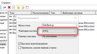
In addition, the useful capacity of the drive depends on the selected file system: FAT16, FAT32, NTFS. Media formatted on different systems will have different usable capacity. This is due to the fact that when formatting a disk, system information about it is written to it and it is different for different file systems.
Well, the last. There is such a phenomenon as a Chinese flash drive: this is when information is deliberately entered into the system partition of a small capacity flash drive that its capacity is large. For example, from 1 GB you can make 32 GB. In practice, if you insert this USB flash drive into a computer, it will show that its capacity is 32 GB. When the user writes data to it in an amount larger than its real one, copying will be completed without errors. But it will be possible to read data from such a carrier in an amount commensurate with the real volume, i.e. no more than 1 GB for our example.


Flash memory belongs to the EEPROM class, but uses a special technology for building memory cells. Erasing in flash memory is performed immediately for the whole area of cells (in blocks or the entire chip). This made it possible to significantly increase the performance in the recording (programming) mode. Flash memory has a combination of high packing density (its cells are 30% smaller than DRAM cells), non-volatile storage, electrical erasing and writing, low consumption, high reliability and low cost ... These are reprogrammable memories.
Like RAM, flash memory is electrically modified internally, but like a ROM, flash is non-volatile and retains data even after a power outage. However, unlike RAM, flash cannot be rewritten byte by byte. Flash memory is being read and written byte by byte and has a new requirement: must be cleared before new data can be written.
Flash memory is semiconductor memory, and a special type. Her elementary cell, which stores one bit of information, is not a capacitor, but field-effect transistor with a special electrically isolated area, which is called the "floating gate". An electric charge placed in this area is able to persist for many years. When writing one bit of data, the cell is charged - the charge is placed on the floating gate, when erasing - the charge is removed from the floating gate and the cell is discharged.
Among such devices, circuits with specialized blocks (asymmetric block structures) are singled out. By the name of the so-called Boot blocks in which information is reliably protected from accidental erasure, memory is called Boot Block Flash Memory.
Flash memory boot block type serves to store up-to-date programs and data in a variety of systems, including cell phones, modems, BIOS, vehicle engine management systems, and more. By using flash memory instead of EEPROM to store parametric data, developers are seeking to reduce the cost and increase the reliability of their systems.
Advantages of flash memory compared to EEPROM:
1.
Higher write speed with sequential access due to the fact that erasing information in flash is done in blocks.
2. The cost of flash memory production is lower due to a simpler organization.
Flaw: Slow writing to arbitrary memory locations.
Memory with serial access Used where data can be queued.
Addressable flash memory. Storing rarely changed data. Recording and erasing is carried out by the processor vych device in the normal operating mode. To do this, Flash memory has an additional control of command words. , written by the processor in a special register of the microcircuit. When a special programming voltage is applied, the circuit ensures the recording and erasing of information. Before programming, the processor reads a code from the chip - an identifier containing the code of the manufacturer and the chip to coordinate the erasing and writing algorithms automatically.
All bytes of the memory or the selected block are erased, after which they are all checked, the erase is performed again and the check is performed.
Memory programming is carried out byte by byte, the recorded information is checked. The processor reads the written byte from the memory and compares it with the original one.
One of the blocks is designed to store the BIOS software and is hardware-protected from accidental erasure.
The principle of operation and the device of flash memory
The memory also contains parameter blocks and master blocks that are not protected against accidental erasure. The main blocks store the main control programs, and the parameter blocks store relatively frequently changed system parameters.
 File Flash
used to replace hard drives. Reduces power consumption, increases the reliability of the memory, reduces their size and weight, increases the speed when reading data. The program can be read by the processor directly from file Flash memory, and the results are also written there.
File Flash
used to replace hard drives. Reduces power consumption, increases the reliability of the memory, reduces their size and weight, increases the speed when reading data. The program can be read by the processor directly from file Flash memory, and the results are also written there.
On the basis of file Flash memory, compact removable external memory devices are created.
SE - MNOP.
2 threshold voltages. Upor1 - has a small value, 1-2 V. When Upor is applied, the m / d drain-source channel is initiated. If there are charges m / d with nitride and silicon dioxide, then Upor increased to 7V.
Writing (programming) flash memory- the process of replacing 1 with 0. Erasing- replacing 0 with 1.
3.RS architecture. computer processors. The structure of processors and their main characteristics. System buses and their characteristics. local tires. Chipsets.
Architecture is a multi-level hierarchy of hardware and software, each of the levels allows for multi-variant construction and application.
Structure is a set of elements and their relationships.
A computer is a complex of hardware and software designed to automate the preparation and solution of user problems.
 Computer architecture- this is a general description of the structure and functions of a computer at a level sufficient to understand the principles of operation and the system of commands of a computer, which does not include details of the technical and physical structure of a computer.
The architecture includes the following principles of computer construction:
1. structure of computer memory;
2. ways to access memory and external devices;
3. the ability to change the configuration;
4. command system;
5. data formats;
6. interface organization.
The architecture of modern personal computers is based on trunk-modular principle. Information communication between computer devices is carried out through system bus(another name is the system highway).
A bus is a cable made up of many conductors. One group of conductors - data bus processed information is transmitted, on the other - address bus- addresses of memory or external devices accessed by the processor. The third part of the highway control bus, control signals are transmitted through it (for example, a signal that the device is ready for operation, a signal to start the device, etc.).
The system bus is characterized clock frequency and bit depth. The number of bits transmitted simultaneously on the bus is called bus width. Clock frequency characterizes the number of elementary data transfer operations per second. The bus width is measured in bits, the clock frequency is measured in megahertz.
System buses
Transfer of information between MP and other elements. Device addressing and the exchange of special service signals are also carried out. The transfer of information on the bus is controlled by one of the devices connected to it or a node specially dedicated for this, called the bus arbiter.
ISA bus(Industry Standard Architecture) has a 36-pin connector for expansion cards. This results in 4 address lines and 8 data lines. 16 bits of data can be transferred in parallel, and 16 MB of system memory can be directly accessed with 24 address lines. Number of hardware interrupt lines - 15.
EISA bus(Extended ISA). provides the largest possible amount of addressable memory, 32-bit data transfer, improved interrupt system, automatic configuration of the system and expansion cards. The EISA connector on the computer's motherboard is ISA compatible. The EISA bus allows addressing 4GB of address space. Theor maximum speed is 33 MB/s. The bus is clocked at a frequency of about 8-10 MHz.
Local buses are designed to increase the speed of the computer, allowing peripheral devices (video adapters, storage controllers) to operate at a clock frequency of up to 33 MHz and higher. An MCA type connector is used.
PCI buses. Between the processor's local bus and the PCI itself there is a special matching circuit
According to the PCI specification, up to 10 devices can be connected to the bus. The PCI bus operates at a fixed clock frequency of 33 MHz and provides both 5 and 3.3 V controller supply voltage, plug and play mode.
PCI-X bus - high performance PCI. is synchronous, i.e. all data is processed simultaneously when a control signal is received. The bus width is 32-bit. At 33 MHz, the theoretical throughput is 132 MB/s.
 Any information transmitted from the processor to other devices on the data bus is accompanied by address transmitted over the address bus. This may be the address of a memory location or the address of a peripheral device. It is necessary that the bus width allows you to transfer the address of the memory cell. Thus, in words, the bus width limits the amount of computer RAM, it cannot be more than , where n is the bus width.
diagram of a computer device built according to the main principle
Chipset- from English. "chip set" - a set of chips designed to work together to perform a set of any functions. So, in computers, the chipset plays the role of a connecting component that ensures the joint functioning of the memory, CPU, input-output and other subsystems. Chipsets are also found in other devices, such as cell phone radios.
The chipset of computer motherboards consists of two main microcircuits (sometimes they are combined into one chip):
- MCH - memory controller hub (Memory Controller Hub) - north bridge (northbridge) - provides interaction of the central processing unit (CPU) with memory and video adapter. Newer chipsets often have an integrated video subsystem.
The memory controller can be integrated into the processor (eg Opteron, Nehalem, UltraSPARC T1).
- ICH - I / O Controller Hub - south bridge (southbridge) - provides interaction between the CPU and hard drive, PCI cards, IDE, SATA, USB interfaces, etc.
Also, sometimes chipsets include the Super I / O chip, which is connected to the south bridge and is responsible for low-speed RS232, LPT, PS / 2 ports.
Currently, the main manufacturers of chipsets for desktop computers are firms. Intel, NVIDIA, AMD(which acquired ATI and currently produces chipsets under its own name), VIA And SIS.
Firm Intel releases chipsets only for its own processors. For company processors AMD chipsets are the most common nVidia(usually marketed under the brand name nForce) and AMD.
Firm chipsets VIA And SIS are popular mainly in the low-end sector, as well as in office systems, although their integrated graphics are significantly inferior to nVidia and AMD in terms of 3D capabilities.
⇐ Previous12345678910Next ⇒
Publication date: 2015-10-09; Read: 262 | Page copyright infringement
Studopedia.org - Studopedia.Org - 2014-2018 year. (0.004 s) ...
Performance comparison of different types of server drives (HDD, SSD, SATA DOM, eUSB)
In this article, we will look at modern server storage models in terms of performance and optimal applications.
At the moment, servers mainly use two types of data storage devices - hard magnetic disks (HDD, hard disk drive) and solid-state drives (SSD, solid-state drive). In addition, devices such as eUSB Flash Module and SATA DOM are also used. Let's consider all these types in more detail.
Modern hard magnetic drives can use one of two interfaces - SATA (Serial Advanced Technology Attachment) and SAS (Serial Attached SCSI). The current version of the SATA interface provides a throughput of 6 Gb / s. Disks with this interface are mainly used in the segment of desktop personal computers, but can also be used in servers. In the server segment, such drives have a spindle speed of 7’200 rpm. The Seagate Constellation.2 ST91000640NS (SATA 7'200, 2.5″) and Seagate Constellation ES ST1000NM0011 (SATA 7'200, 3.5″) models will take part in our testing of drives of this type.
A more reliable and productive disk SAS interface is designed for server solutions and workstations. It also has a bandwidth of up to 6 Gb / s, but already in Full Duplex mode, which means that data can be transmitted simultaneously in both directions at a speed of 6 Gb / s. Drives with this interface have a higher MTBF (Mean Time Between Failures, mean time between failures). Moreover, the SAS interface, unlike SATA, uses a different instruction set with support for a higher request queue depth (64 versus 32, the greater the queue depth, the better the optimization of the request execution order) and dual-port connectivity for possible fault tolerance. An important feature of SAS is a more adapted connection of SAS disks to various backplanes, cages, expanders, RAID and HBA controllers, data storage systems and other devices both via internal and external ports. Currently, servers use SAS disks with a spindle speed of 7'200, 10'000 and 15'000 rpm.
Speed 7’200 rpm. was initially atypical for the server segment, however, hard drive manufacturers at some point decided to produce drives with a rotation speed of 7,200 rpm not only with the SATA interface, but also with the SAS interface. In their "mechanical" part, these drives are exactly the same, they differ only in the way they are connected. The move increased the affordability of SAS drives and provided the server segment with larger SAS drives. The main area of application of such disks is low-budget workstations and entry-level servers. The tested drives of this type are Seagate Constellation.2 ST91000640NS (SAS 7'200, 2.5″) and Seagate Constellation ES.3 ST1000NM0023 (SAS 7'200, 3.5″).
10,000 RPM SAS drives are a good solution for powerful workstations and low-cost enterprise-class server solutions. The tested disk is Seagate Savvio 10K5 ST9900805SS (SAS 10000 2.5″).
15,000 RPM SAS drives are the best choice for enterprise servers, data centers (DPCs) and storage systems (SANs). The tested disk is Seagate Cheetah 15K7 ST3300657SS (SAS 15000 3.5″).
The performance of the above drives on sequential and random read/write operations is shown in the following diagram.

At the same spindle speed and physical platter size, SAS drives are faster than SATA drives, which is explained by the higher linear data density of SAS drives compared to SATA drives.
On the other hand, the SAS 7'200, 3.5" drive and the SAS 10'000, 2.5" drive show almost the same results. This is explained by the fact that the advantage in rotation speed is compensated by the smaller physical size of the disk platters 2.5”, as a result of which, with the same linear data density, the linear speed of the heads relative to the platters is approximately the same.

In the random read test, which measures input/output operations per second (IOPS), 2.5” 7'200 rpm drives perform better than 3.5” drives of the same speed, because "small" drives moving the head to the desired sector is less. SAS drives here again show a higher result compared to SATA drives, this time due to better optimization of the random request execution queue due to support for a higher queue depth (64 for SAS versus 32 for SATA). The advantage of 10,000 and 15,000 rpm SAS drives is not only due to the high spindle speed, but also because they have a more advanced head positioning mechanism with less access time.
On random write operations, SAS drives have the same advantage over SATA drives as they do on read operations.
Solid-state drives using NAND-Flash non-volatile memory have hundreds of times faster random read and write speeds than hard drives because the magnetic head does not need to be moved in SSDs. In addition, the SSD has less power consumption and no noise during operation. But they also have disadvantages, namely: high cost and relatively small volume compared to HDD. In the desktop PC segment, such drives are used in conjunction with the HDD according to the scheme when the operating system and the most necessary programs are installed on the SSD, and all other data is stored on the HDD. This approach significantly increases the speed of the computer, without greatly increasing its cost. For testing, we chose an Intel 520 Series 240GB drive. This drive is recommended for use in desktops, laptops and workstations.
In the server segment, the situation with SSDs is significantly different. Placing large amounts of data on an SSD is quite expensive. But they can be successfully used for caching, when the SSD cache is used to allocate "hot" data, that is, data that is accessed most often. This gives a huge performance boost to the server's disk subsystem, especially for random access operations. The tested server SSD is an Intel DC S3700 100GB.

With sequential reading, desktop and server drives show almost the same results, but with sequential writing, the server type of SSD noticeably loses. This is due to the fact that the server drive uses memory that allows an order of magnitude more write cycles, but the write operations themselves are slower.

On random write operations, the lag is also significant, but this is due to the need to provide a much larger write resource for server drives.
eUSB drives, like SSDs, also use Flash modules for data storage, but they are installed directly into the USB connector on the server motherboard. Such drives have a number of functional and other limitations due to the use of the USB port as an interface. Loading a full version of Windows OS does not work from such a drive, and the interface speed (480 Mbps) is much lower than that of SATA (6 Gbps). The most optimal area for their application in servers is the use of a small operating system as a bootloader, for example, the VMware ESXi hypervisor.
Thin clients use these drives to store an image of the Windows Embedded operating system. The tested drive is eUSB Transcend 4GB.
SATA DOM drives are more functional than eUSB drives. They are connected in the same way as SSD drives, to the SATA connector, but at the same time they “look” more like a USB drive than a hard drive.
The device and principle of operation of a flash drive
They are installed directly into the SATA connectors on the motherboard of a computer or server. It is convenient when such a connector has built-in power, otherwise it has to be provided through an additional cable. Considering that these drives are connected to standard SATA connectors, the BIOS of the motherboard works with them as with ordinary HDD or SSD drives, which makes it possible to install a full bootable version of the Windows operating system on the SATA DOM. In the server, this frees up space in the disk subsystem's bucket, allowing it to be used for the RAID disk. In addition, the SATA DOM drive is located inside the server platform, which prevents accidental removal of the disk with the installed OS. Such drives can be used in the desktop and server segments, as well as in thin clients, by installing any operating system or hypervisor for virtualization. The tested drive is SATA DOM Innodisk 8 GB.

The test results of eUSB-Flash and SATA DOM drives are consistent with the performance of their interfaces. According to the USB 2.0 specification, the speed is 25 - 480 Mbps, and for SATA 3.0 - 6,000 Mbps, which already inclines the choice in favor of devices with a SATA interface. On the graph, we see a 2.5 times superiority in SATA DOM Innodisk sequential read and write operations over eUSB-Flash.

In the test of random read operations, the situation does not change, SATA DOM is also in the lead. Random writes for both drives are equally at a very low level, but they are not intended for these operations.
The performance data of the best representatives of each type of drives from our testing are shown in the following charts. The solid-state drive from Intel shows itself as a clear leader.


We hope that our article will help you decide on the choice of a particular drive. And there really is plenty to choose from. A wide variety of drives are offered by manufacturers, but to achieve the best results, you need to properly plan your needs and expectations from storage subsystems.
Measurements for HDD and SSD were carried out on the same Intel RS25DB080 controller. Testing was performed using the IOmeter program with the following parameters: the controller and disk caches are disabled, the command queue depth is 256, the Strip Size parameter is 256KB, the data block size is 256KB for sequential operations and 4KB for random operations. The speed of sequential operations was measured in MB / s, random - in IOPS (the number of input / output operations per second).
Server hardware department engineer Andrey Leontiev
03.06.13
Mach Xtreme Technology, a Taiwanese company specializing in high-performance computer components and heavily involved in the production of solid state drives, has launched retail sales of an advanced storage solution called PCIe SSD MX-EXPRESS.
Flash memory. Past, present and future
The novelty has a low-profile design, is characterized by the following overall dimensions: 152.5 x 19 x 69 mm, weight - 125 grams, connects to a computer via a PCI-Express 2.0 x2 slot, uses an as yet unnamed dual controller and is available in four versions in terms of volume: 128 GB, 256 GB, 512 GB and 1 TB.

The drive has support for ROHS, CE and FCC certificates, it does not require any drivers to install into the system. The data transfer speed varies depending on the capacity of the discs. So, for 512-GB and 1-TB solutions, the sequential read speed is 850 Mb / s, and the write speed is 800 Mb / s, the performance level is in the region of 100,000 IOPS, and the access time is 0.1 ms.
MX-Express series drives have a huge lifespan of 2.5 million hours, can operate at ambient temperatures from zero to 70 degrees Celsius, support TRIM, DuraClass, DuraWrite, RAISE and Garbage Collector. In addition, the new product comes with a low-profile PCI plug.

The 128 GB model will cost everyone 309.90 euros, 256 GB - 379.90 euros, 512 GB - 669.90 euros and 1 TB - 1449.90 euros. The manufacturer's quality guarantee for the devices is 2 years.
I am constantly faced with the fact that the confusion in the term flash drive, often becomes a cause of misunderstanding between the buyer and the seller when choosing the necessary storage medium. So, "in the broad masses" there are the following main interpretations of the word flash drive: USB flash drive(USB flash drive), memory card microSD(read micro-eS-Di), in general, any memory card, in general, any flash-media. Here under the word flash(read flash) I mean flash memory technology and use the English term so that there is no confusion. Moreover, I sometimes see that people in everyday life can simultaneously call any of these devices a flash drive, relying on the fact that their interlocutor, by context or with the help of telepathy, will understand what it is about!
I will not argue about which term is more correct, and even more so I will skip the question of how “flash” or “flash” is correct (in fact, both spellings are used at least the same way, and nothing can be done about it). Instead of unnecessary disputes, I will simply describe all the devices called by this word, and all the words they are called, and then you can definitely buy exactly what you need!
So let's start with USB flash drive. It is behind this device, which is a universal medium containing flash memory and connected directly to the USB connector, that the word flash drive has stuck in Russian. However, the word flash drive or flash drive, derived from the English Flash Drive, is also popular, as well as the more semi-official flash drive (or flash drive). Since it is impossible to come up with a reasonable translation of this phrase (well, do not call the flash drive a "flickering driver"!), The words flash drive or flash drive should be recognized as the best term. Here are typical examples of flash drives:
Flash drives are mainly used to transfer information between computers. Or to store information that you always want to have with you. Since we are talking about typology, I note that recently there have been flash drives with a connection USB3.0. What does it mean? This means that if the computer has a USB3.0 interface (its most noticeable external difference is blue), the USB3.0 flash drive will be able to work faster. If you connect it to a traditional USB2.0 (which is on every computer), then its speed will be comparable to the speed of a conventional flash drive. This is what USB3.0 and USB2.0 look like:  Now the second category of devices called flash drives: microSD cards(or microSDHC, their immediate successors)
  According to my observation, they are called flash drives either by those who did not hold any other flash media in their hands (and this is no wonder, because microSD / microSDHC are used in almost all phones, players and all sorts of gadgets there), or those who have other names for all this " little things" does not know. They also contain flash memory, which means they have the right to be called flash drives. But for understanding between people, it is desirable to somehow differentiate the concepts, so the “memory card” will sound more preferable, especially if you need to explain to the seller what you need. It is also important to know that memory cards are different! So it's nice to add: "such a small memory card", but here you can get into trouble: there are M2 memory cards that are very similar in size. Fortunately, they are used only in Sony products. We will mention them below. But still, it is better to remember the magic words microSD and microSDHC (read microesDe and microesDeHaTse). In colloquial speech, by the way, most often the first word (microSD) is used to refer to both types of cards (both microSD and microSDHC). There is nothing wrong with that.
What you need to know about microSD and microSDHC memory cards? First, how are they different? microSDHC is a newer standard that supports more than 4 gigabytes of storage. All memory cards over 4 GB can only be microSDHC, and less than 4 can only be microSD. But 4 GB is not lucky: they can be like this and that! However, 4 GB microSD is a rarity. Now the most important question: how to choose the one that suits your device? There are two rules: firstly, you need to determine the maximum size of the memory card that your device can work with (to do this, open the instructions for it, or use the search on the Internet). Secondly, you need to buy a card that is the same or smaller than the maximum amount. Moreover, all devices that support microSDHC will work with any microSD card of any size. There is only one nuance here: if your device is indicated that it supports a card no more than 4 GB, then this may mean that it does not support any microSDHC cards and supports any microSD cards, including 4 GB. Or it may mean that it supports any 4 GB cards, both microSD and microSDHC, but does not support 8 GB microSDHC cards and above. Here is the arithmetic. And if there are no clarifications in the instructions about this, then you will have to use the good old “scientific poke method”.
Now another important characteristic that is often of interest to buyers: what kind of Class specified for microSDHC cards? It is denoted by a number inside the English letter C.  I must say right away that this is not a variety like, say, tomatoes. Memory card class is its ability to write information at some minimum guaranteed speed. The higher the class, the higher the speed. Moreover, this is precisely the guaranteed smallest speed, while the maximum and average speeds can be significantly higher. Two cards of different classes can often have almost the same average and maximum write speeds, but if one of them has “gaps” in speed, that is, sometimes writes more slowly, then it will have a lower class. In other words: the class guarantees that the speed of the card in any part of the recording does not fall below a certain threshold. Why is it needed? The class is needed for devices that write information quickly and cannot wait. These are mainly video cameras that need to record video, because if the memory card does not have time to record a frame during its shooting, then the “train will leave”: you will need to write the next frame, followed by the next and some part of the information the camera will have to “throw out” ”, which will adversely affect the quality of the shooting. So, again, we take the instruction and see what it says about the class of the memory card. If nothing - you can save money, if the class is indicated - take the specified one or higher.
Finally, the last thing you need to decide when buying a microSD / microSDHC memory card is an adapter or adapter to SD. This thing is 4 times the size of the card itself, with the help of which your micro card turns into a "large" SD / SDHC card (see below about them). Some cards are sold with an adapter, some without.  Evaluate whether you need such an adapter, taking into account the devices you have: cameras, old e-books, etc. And also do not forget about your card reader: maybe it does not read micro cards directly and then the adapter will not bother you at all. In general, the adapter expands your capabilities in "just in case". On the other hand: will you find it when you need it in your desk? The choice is yours.
Now let's move on to SD/SDHC cards.  I won't talk much about them: these are the older brothers of microSD/microSDHC cards. Everything that has been said about those is also true for these oversized ones (although the "micro" cards are more likely to be undersized, because at first they were large, and then their smaller counterparts appeared). The only thing is that they don’t have adapters, since they don’t need to be adapted to themselves, well, they are used in more voluminous devices - these are, first of all, soap cameras and all sorts of electronic books (although the latter are increasingly equipped with microSDHC cards ).
M2. Full name Memory Stick micro M2- these are cards very similar to microSD / microSDHC.  They differ in that they are used in phones and players of the company Sony, It would be more correct to say “used”, because Sony finally realized that “one man is not a warrior” and began to use the formats of the SD line. If you are a happy owner of Sony, be careful, check what card you have! These cards do not have any classes.
The last card we'll look at is compact flash(in Russian it is pronounced “compact flash”, but it is almost always written in English, probably because writing “compact” about the largest card on the market today is somehow not literary :-).  These cards, due to their decent size, have their undoubted advantages: the capacity is many times greater than that of other cards and the speed that is still unattainable for SDHC memory cards. Therefore, they are used in large "advanced" cameras and other demanding devices. It remains to add that the speed (this time without the "intricacies" with a guaranteed minimum) is indicated by a number and the letter X. For example: 133x, 266x, 300x. The number indicates how many times this card is faster than some minimum standard CD-reading speed.
If you have not found your favorite prehistoric map in this review - do not worry! You will definitely find it on Wikipedia. I deliberately limited myself to only the types of flash media that are common today, so as not to fill anyone's head with unnecessary information and not turn the article into an archivist. So, now you are armed with knowledge, and choosing the right flash drive will not be a problem for you. Enjoy the shopping!
Foreword
The New Year is a pleasant, bright holiday, on which we all sum up the results of the past year, look to the future with hope and give gifts. In this regard, I would like to thank all habr-residents for their support, help and interest in my articles (, , ,). If you had not once supported the first one, there would have been no subsequent ones (already 5 articles)! Thanks! And, of course, I want to make a gift in the form of a popular science and educational article about how fun, interesting and beneficial (both personal and public) can be used, rather harsh at first glance, analytical equipment. Today, on New Year's Eve, on the festive operating table are: a USB-Flash drive from A-Data and a SO-DIMM SDRAM module from Samsung.Theoretical part
I will try to be as brief as possible so that we all have time to prepare Olivier salad with a margin for the festive table, so part of the material will be in the form of links: if you want, read at your leisure ...What kind of memory is there?
At the moment, there are many options for storing information, some of them require a constant supply of electricity (RAM), some are permanently "sewn" into the control microcircuits of the technology around us (ROM), and some combine the qualities of those and others (Hybrid). Flash belongs to the latter, in particular. It seems to be non-volatile memory, but the laws of physics are difficult to cancel, and periodically you still have to rewrite information on flash drives.The only thing that, perhaps, can unite all these types of memory is more or less the same principle of operation. There is some two-dimensional or three-dimensional matrix, which is filled with 0 and 1 approximately in this way and from which we can subsequently either read these values or replace them, i.e. all this is a direct analogue of the predecessor - memory on ferrite rings.
What is flash memory and what is it like (NOR and NAND)?
Let's start with flash memory. Once upon a time, on the notorious ixbt, quite a bit was published about what Flash is, and what 2 main varieties of this type of memory are. In particular, there is NOR (logical not-or) and NAND (logical not-and) Flash memory (everything is also described in great detail), which differ somewhat in their organization (for example, NOR is two-dimensional, NAND can be three-dimensional), but they have one common element - a floating gate transistor.
Schematic representation of a floating gate transistor.
So how does this marvel of engineering work? Together with some physical formulas, this is described. In short, between the control gate and the channel through which the current flows from the source to the drain, we place the same floating gate, surrounded by a thin layer of dielectric. As a result, when current flows through such a “modified” FET, some of the high-energy electrons tunnel through the dielectric and end up inside the floating gate. It is clear that while the electrons were tunneling and wandering inside this gate, they lost some of their energy and practically cannot return back.
NB:“practically” is the key word, because without overwriting, without updating cells at least once every few years, Flash is “zeroed” just like RAM, after the computer is turned off.
Again, we have a two-dimensional array that needs to be filled with 0s and 1s. Since it takes quite a long time to accumulate charge on the floating gate, a different solution is applied in the case of RAM. The memory cell consists of a capacitor and a conventional field effect transistor. At the same time, the capacitor itself has, on the one hand, a primitive physical device, but, on the other hand, it is non-trivially implemented in hardware:

RAM cell device.
Again, ixbt has a good one dedicated to DRAM and SDRAM memory. It is, of course, not so fresh, but the fundamental points are described very well.
The only question that torments me is: can DRAM have, like flash, a multi-level cell? It seems so, but still...
Part practical
Flash
Those who have been using flash drives for a long time have probably already seen a “naked” drive, without a case. But I will still briefly mention the main parts of a USB flash drive:
The main elements of a USB-Flash drive: 1. USB connector, 2. controller, 3. PCB-multilayer printed circuit board, 4. NAND memory module, 5. reference frequency crystal oscillator, 6. LED indicator (now, however, on many flash drives do not have it), 7. a write protection switch (similarly, many flash drives do not have it), 8. a place for an additional memory chip.
Let's go from simple to complex. Crystal oscillator (more on the principle of operation). To my deep regret, during the polishing, the quartz plate itself disappeared, so we can only admire the case.

Crystal oscillator housing
By chance, in the meantime, I found what the reinforcing fiber looks like inside the textolite and the balls that make up the textolite for the most part. By the way, the fibers are still laid with a twist, this is clearly seen in the top image:

Reinforcing fiber inside the textolite (red arrows indicate fibers perpendicular to the cut), of which the bulk of the textolite consists
And here is the first important part of the flash drive - the controller:

Controller. The top image was obtained by combining several SEM micrographs.
To be honest, I didn’t quite understand the idea of the engineers who placed some additional conductors in the chip filling itself. It may be easier and cheaper to do this from the point of view of the technological process.
After processing this picture, I shouted: “Yaaaaaaz!” and ran around the room. So, the 500 nm process technology is presented to your attention in all its glory with perfectly traced boundaries of the drain, source, control gate, and even the contacts have been preserved in relative integrity:

"Ide!" microelectronics - 500 nm controller process technology with beautifully traced separate drains (Drain), sources (Source) and control gates (Gate)
Now let's get down to dessert - memory chips. Let's start with the contacts that feed this memory in the truest sense of the word. In addition to the main (in the figure the “thickest” contact) there are also many small ones. By the way, "fat"< 2 диаметров человеческого волоса, так что всё в мире относительно:

SEM images of pins powering the memory chip
If we talk about memory itself, then success awaits us here too. It was possible to shoot individual blocks, the boundaries of which are marked with arrows. Looking at the image at maximum magnification, try to strain your eyes, this contrast is really hard to distinguish, but it is on the image (for clarity, I marked a separate cell with lines):

Memory cells 1. Block boundaries are marked with arrows. Lines represent individual cells
At first it seemed to me as an artifact of the image, but after processing all the photos at home, I realized that these are either control shutters elongated along the vertical axis with an SLC cell, or these are several cells assembled in an MLC. Although I mentioned MLC above, it is still a question. For reference, the "thickness" of the cell (i.e. the distance between the two bright dots in the bottom image) is about 60 nm.
In order not to dissemble - here are similar photos from the other half of the flash drive. Completely similar picture:

Memory cells 2. Block boundaries are marked with arrows. Lines represent individual cells
Of course, the chip itself is not just a set of such memory cells, there are some other structures inside it, the belonging of which I could not determine:

Other Structures Inside NAND Memory Chips
DRAM
Of course, I did not cut the entire SO-DIMM board from Samsung, I only “disconnected” one of the memory modules with the help of a building hair dryer. It is worth noting that one of the tips proposed even after the first publication came in handy here - sawing at an angle. Therefore, for a detailed immersion in what he saw, this fact must be taken into account, especially since the cut at 45 degrees made it possible to obtain, as it were, “tomographic” sections of the capacitor.However, according to tradition, let's start with contacts. It was nice to see what the BGA “chipped” looks like and what the soldering itself is:

"Skol" BGA-soldering
And now it’s time to shout “Ide!” for the second time, as we managed to see individual solid-state capacitors - concentric circles in the image, marked with arrows. It is they who store our data while the computer is running in the form of a charge on their plates. Judging by the photographs, the dimensions of such a capacitor are about 300 nm wide and about 100 nm thick.
Due to the fact that the chip is cut at an angle, some capacitors are cut neatly in the middle, while others have only “sides” cut off:

DRAM memory at its finest
If someone doubts that these structures are capacitors, then you can see a more “professional” photo (though without a scale mark).
The only thing that confused me is that the capacitors are arranged in 2 rows (lower left photo), i.e. it turns out that there are 2 bits of information per 1 cell. As mentioned above, there is information on multi-bit recording, but how applicable and used this technology is in modern industry remains a question for me.
Of course, in addition to the memory cells themselves, there are also some auxiliary structures inside the module, the purpose of which I can only guess:

Other Structures Inside a DRAM Chip
Afterword
In addition to those links that are scattered throughout the text, in my opinion, this review is quite interesting (albeit from 1997), the site itself (and the photo gallery, and chip-art, and patents, and many, many things) and this office, which actually engaged in reverse engineering.Unfortunately, we could not find a large number of videos on the production of Flash and RAM, so you will have to be content with assembling USB-Flash drives:
P.S.: Once again, Happy New Year of the Black Water Dragon!!!
It turns out strange: I wanted to write an article about Flash one of the first, but fate decreed otherwise. Fingers crossed, let's hope that the next, at least 2, articles (about bio-objects and displays) will be published in early 2012. In the meantime, the seed is carbon tape:

Carbon tape on which the test samples were fixed. I think normal duct tape looks the same.
A modern person likes to be mobile and carry various high-tech gadgets (eng. gadget - a device) that make life easier, but what is there to hide, making it more intense and interesting. And they appeared in just 10-15 years! Small, light, handy, digital... All this gadgets have achieved thanks to new microprocessor technologies, but still the greatest contribution was made by one remarkable storage technology, which we will talk about today. So, flash memory.
There is an opinion that the name FLASH in relation to the type of memory is translated as "flash". Actually this is not true. One of the versions of its appearance says that for the first time in 1989-90, Toshiba used the word Flash in the context of "fast, instantaneous" when describing its new chips. In general, Intel is considered the inventor, which introduced flash memory with the NOR architecture in 1988. A year later, Toshiba developed the NAND architecture, which is still used today along with the same NOR in flash chips. Actually, now we can say that these are two different types of memory that have somewhat similar production technology. In this article, we will try to understand their device, how they work, and also consider various options for practical use.
NOR
With the help of it, the input voltages are converted into output voltages corresponding to "0" and "1". They are necessary because different voltages are used to read/write data in a memory cell. The cell scheme is shown in the figure below.


It is typical for most flash chips and is a transistor with two insulated gates: control (control) and floating (floating). An important feature of the latter is the ability to hold electrons, that is, charge. Also in the cell there are so-called "drain" and "source". When programming between them, due to the influence of a positive field on the control gate, a channel is created - a flow of electrons. Some of the electrons, due to the presence of more energy, overcome the insulator layer and enter the floating gate. On it they can be stored for several years. A certain range of the number of electrons (charge) on the floating gate corresponds to a logical unit, and everything that is greater than it is zero. When reading, these states are recognized by measuring the threshold voltage of the transistor. To erase information, a high negative voltage is applied to the control gate, and the electrons from the floating gate pass (tunnel) to the source. In technologies from different manufacturers, this principle of operation may differ in the way current is applied and data is read from the cell. I also want to draw your attention to the fact that in the structure of flash memory, only one element (transistor) is used to store 1 bit of information, while in volatile types of memory this requires several transistors and a capacitor. This makes it possible to significantly reduce the size of manufactured microcircuits, simplify the technological process, and, consequently, reduce the cost. But even one bit is far from the limit: Intel is already releasing StrataFlash memory, each cell of which can store 2 bits of information. In addition, there are trial samples, with 4 and even 9-bit cells! This memory uses the technology of multi-level cells. They have the usual structure, and the difference lies in the fact that their charge is divided into several levels, each of which is assigned a certain combination of bits. Theoretically, more than 4 bits can be read / written, however, in practice, problems arise with the elimination of noise and with the gradual leakage of electrons during prolonged storage. In general, the memory chips that exist today for cells are characterized by the storage time of information, measured in years, and the number of read / write cycles - from 100 thousand to several million. Among the shortcomings, in particular, of NOR flash memory, it is worth noting poor scalability: it is impossible to reduce the area of chips by reducing the size of transistors. This situation is related to the way the matrix of cells is organized: in the NOR architecture, an individual contact must be connected to each transistor. Flash memory with NAND architecture is much better in this regard.
NAND

The device and principle of operation of the cells is the same as that of NOR. Although, in addition to logic, there is still one more important difference - the architecture of the placement of cells and their contacts. Unlike the case described above, here there is a contact matrix, in the intersections of rows and columns of which transistors are located. This is comparable to a passive matrix in displays :) (and NOR - with an active TFT). In the case of memory, such an organization is somewhat better - the area of \u200b\u200bthe microcircuit can be significantly reduced due to the size of the cells. Disadvantages (where without them) are lower compared to NOR speed in byte-by-byte random access operations.
There are also such architectures as: DiNOR (Mitsubishi), superAND (Hitachi), etc. They do not represent anything fundamentally new, but only combine the best properties of NAND and NOR.
And yet, be that as it may, NOR and NAND are currently produced on an equal footing and practically do not compete with each other, because, due to their qualities, they are used in different areas of data storage. This will be discussed further...
Where memory is needed...
The scope of any type of flash memory depends primarily on its speed performance and reliability of information storage. The NOR memory address space allows you to work with individual bytes or words (2 bytes). In NAND, cells are grouped into small blocks (similar to a hard disk cluster). From this it follows that with sequential reading and writing, NAND will have the advantage in speed. However, on the other hand, NAND loses significantly in random access operations and does not allow you to work directly with bytes of information. For example, to change one byte requires:
- read into the buffer the block of information in which it is located
- change the desired byte in the buffer
- write the block with the changed byte back
If we add block fetch and access delays to the execution time of the listed operations, we will get indicators that are by no means competitive with NOR (I note that it is for the case of byte-by-byte recording). Sequential write / read is another matter - here NAND, on the contrary, shows significantly higher speed characteristics. Therefore, and also because of the possibilities of increasing the amount of memory without increasing the size of the microcircuit, NAND flash has found application as a store of large amounts of information and for its transfer. The most common devices based on this type of memory today are flash drives and memory cards. As for the NOR flash, chips with such an organization are used as program code custodians (BIOS, RAM of handheld computers, mobile phones, etc.), sometimes they are implemented as integrated solutions (RAM, ROM and processor on one mini-board, and even in one chip). A good example of this use is the Gumstix project: a single-board computer the size of a stick of gum. It is NOR chips that provide the level of information storage reliability required for such cases and more flexible options for working with it. The volume of a NOR flash is usually measured in units of megabytes and rarely exceeds tens.
And there will be a flash ...
Of course, flash is a promising technology. However, despite high growth rates, storage devices based on it are still expensive enough to compete with desktop or laptop hard drives. Basically, now the sphere of dominance of flash memory is limited to mobile devices. As you understand, this segment of information technology is not so small. In addition, according to the manufacturers, the flash expansion will not stop there. So, what are the main development trends in this area.
First, as mentioned above, a lot of attention is paid to integrated solutions. Moreover, projects like Gumstix are only intermediate stages on the way to the implementation of all functions in one chip.

So far, the so-called on-chip (single-chip) systems are combinations in one flash memory chip with a controller, processor, SDRAM, or with special software. So, for example, Intel StrataFlash in combination with Persistent Storage Manager (PSM) software makes it possible to use the amount of memory both for storing data and for executing program code. PSM is essentially a file system supported by Windows CE 2.1 and above. All this is aimed at reducing the number of components and reducing the size of mobile devices while increasing their functionality and performance. No less interesting and relevant is the development of Renesas - superAND flash memory with built-in control functions. Up to this point, they were implemented separately in the controller, but now they are integrated directly into the chip. These are the functions of bad sectors control, error correction (ECC - error check and correct), cell wear uniformity (wear leveling). Since they are present in one form or another in most other branded firmware for external controllers, let's take a quick look at them. Let's start with bad sectors. Yes, they are also found in flash memory: chips with an average of up to 2% of non-working cells are already leaving the assembly line - this is a common technological norm. But over time, their number may increase (the environment should not be particularly blamed for this - electromagnetic, physical (shaking, etc.) influence is not terrible for a flash chip). Therefore, just like hard drives, flash memory has a reserve capacity. If a bad sector appears, the control function replaces its address in the file allocation table with the sector address from the spare area.
 |
 |
Actually, the ECC algorithm is engaged in identifying bads - it compares the recorded information with the actually recorded one. Also, due to the limited resource of the cells (on the order of several million read / write cycles for each), it is important to have a function to take into account the uniformity of wear. I will give such a rare but occurring case: a keychain with 32 MB, of which 30 MB are occupied, and something is constantly being written and deleted to the free space. It turns out that some cells are idle, while others are intensively depleting their resource. To prevent this from happening, in branded devices, free space is conditionally divided into sections, for each of which the control and accounting of the number of write operations is carried out.
Even more complex all-in-one configurations are now widely represented by companies such as Intel, Samsung, Hitachi, etc. Their products are multifunctional devices implemented in a single microcircuit (standardly, it has a processor, memory and SDRAM). They are focused on the use in mobile devices, where high performance is important with minimal size and low power consumption. These include: PDA, smartphones, phones for 3G networks. I will give an example of such developments - a chip from Samsung, which combines an ARM processor (203 MHz), 256 MB of NAND memory and 256 SDRAM. It is compatible with common operating systems: Windows CE, Palm OS, Symbian, Linux and has USB support. Thus, on its basis, it is possible to create multifunctional mobile devices with low power consumption, capable of working with video, sound, voice and other resource-intensive applications.
Another way to improve flash is to reduce power consumption and size while increasing the amount and speed of memory. To a greater extent, this applies to chips with NOR architecture, since with the development of mobile computers that support wireless networks, NOR flash, due to its small size and low power consumption, will become a universal solution for storing and executing program code. Soon, 512 Mbps NOR chips of the same Renesas will be put into serial production. Their supply voltage will be 3.3 V (let me remind you that they can store information without current supply), and the speed in write operations is 4 MB / s. At the same time, Intel is already introducing its StrataFlash Wireless Memory System (LV18/LV30), a versatile flash memory system for wireless technology. Its memory capacity can reach 1 Gbit, and the operating voltage is 1.8 V. Chip manufacturing technology is 0.13 nm, plans are to switch to 0.09 nm process technology. Among the innovations of this company, it is also worth noting the organization of a batch mode of operation with NOR-memory. It allows you to read information not by one byte, but by blocks of 16 bytes: using a 66 MHz data bus, the speed of information exchange with the processor reaches 92 Mbps!
Well, as you can see, technology is developing rapidly. It is possible that by the time the article is published, something new will appear. So, if anything - do not charge :) I hope you were interested in the material.